Eureka AIR delivers breakthrough ideas for toughest innovation challenges, trusted by R&D personnel around the world.

Manufacturing method of semiconductor element

A manufacturing method and semiconductor technology, applied in semiconductor/solid-state device manufacturing, semiconductor devices, electrical components, etc., can solve problems such as large resistance displacement distribution, capacitor bridging, short circuit, etc., to reduce sidewall protrusions, avoid bridging, and control The effect of silhouette

Active Publication Date: 2013-10-02
UNITED MICROELECTRONICS CORP
View PDF3 Cites 0 Cited by
  • Summary
  • Abstract
  • Description
  • Claims
  • Application Information

AI Technical Summary

Problems solved by technology

[0003] For example, in a metal-insulator-metal capacitor, the performance of the stress migration (SM) of the metal electrode is not good, and the resistance displacement distribution is too large, which will seriously affect the charge storage characteristics of the capacitor.
The gap between the capacitors becomes smaller, and if the etching residue is left between two adjacent capacitors, it may cause capacitor bridging problems
In addition, if the electrode profile of the capacitor is not properly controlled, it may cause short circuit problems

Method used


Image

  • Manufacturing method of semiconductor element
  • Manufacturing method of semiconductor element
  • Manufacturing method of semiconductor element

Examples


Embodiment Construction

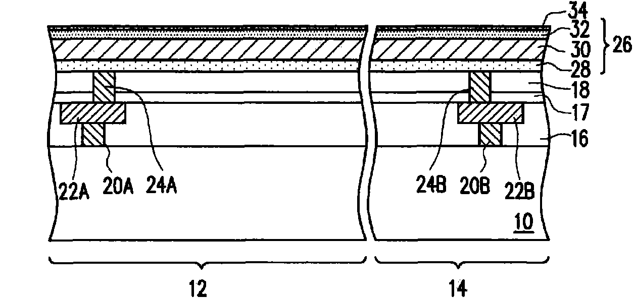
[0038] Figures 1A to 1G It is a schematic cross-sectional view of a process flow of a method for manufacturing a semiconductor device according to an embodiment of the present invention.

[0039] Please refer to Figure 1A As shown, the substrate 10 includes a first circuit area 12 and a second circuit area 14 . The first circuit area 12 is, for example, a core circuit area; the second circuit area 14 is, for example, a logic circuit area. A dielectric layer 16 and a dielectric layer 18 have been formed on the first circuit area 12 and the second circuit area 14 of the substrate 10 . The dielectric layer 16 on the first circuit area 12 has a via plug 20A and a wire 22A; the dielectric layer 18 on the first circuit area 12 has a via plug 24A in it. The dielectric layer 16 on the second circuit area 14 has a via plug 20B and a wire 22B; the dielectric layer 18 on the second circuit area 14 has a via plug 24B in it. Transistors, other dielectric layers, via plugs, metal wires...


PUM

PropertyMeasurementUnit
thicknessaaaaaaaaaa
thicknessaaaaaaaaaa

Abstract

The invention relates to a manufacturing method of a semiconductor element, which comprises the following steps of: firstly, forming a lower electrode material layer containing aluminum and copper on a substrate; secondly, forming an insulating material layer and an upper electrode material layer on the surface of the lower electrode material layer in sequence; thirdly, forming a patterned photoresist layer on the upper electrode material layer, and patterning the upper electrode material layer by using the photoresist layer as a mask to form a patterned upper electrode material layer; fourthly, ashing and removing the patterned photoresist layer by using a plasma, and fusing the patterned lower electrode material layer; and finally, patterning the insulating material layer and the lower electrode material layer to form a patterned insulating layer and a lower patterned electrode layer.

Description

technical field [0001] The present invention relates to a manufacturing method of an integrated circuit, and in particular to a manufacturing method of a semiconductor element. Background technique [0002] In order to meet the needs of the market for lightness, thinness, shortness, and smallness, the semiconductor process is constantly evolving to a smaller line width. However, after the line width shrinks, the resistance value of each material layer, the outline of the pattern and the control of defects will become more important. [0003] For example, in a metal-insulator-metal capacitor, the stress migration (SM) performance of the metal electrode is not good, and the resistance displacement distribution is too large, which will seriously affect the charge storage characteristics of the capacitor. The gap between the capacitors becomes smaller, and etch residues left between two adjacent capacitors can cause capacitor bridging problems. In addition, if the electrode pr...

Claims


Application Information

Patent Timeline
Patent Type & Authority Patents(China)
IPC IPC(8): H01L21/02H01L21/28
Inventor 徐俊成
Owner UNITED MICROELECTRONICS CORP
Why Eureka
Eureka Blog
Learn More