LED surface mounting structure for silicon substrate integrated with functional circuits and packaging method thereof

A technology of LED packaging and functional circuits, applied in circuits, electrical components, electric solid devices, etc., can solve problems such as unsatisfactory heat dissipation, difficult miniaturization, poor temperature resistance, etc., to achieve high integration and reduce Process cost and process difficulty, the effect of packaging cost reduction

Inactive Publication Date: 2011-01-26
APT ELECTRONICS
View PDF4 Cites 35 Cited by
  • Summary
  • Abstract
  • Description
  • Claims
  • Application Information

AI Technical Summary

Problems solved by technology

However, the current LED surface mount structure has the following problems: since the packaging bracket 100 uses a metal bracket as the substrate, and then is sealed and cut by injecting plastic grooves or molding, its temperature resistance is not good. Good, heat dissipation is not ideal, miniaturization is not easy to manufacture
In addition, LED peripheral circuits also include rectifier circuits (i.e. AC-DC conversion circuits), dimming circuits, load monitoring and diagnosis, etc. These functional circuits are packaged separately, large in size and high in cost, but these circuits are actually integrated silicon process Circuit, if part of the circuit can be integrated in the silicon substrate, it will effectively increase the integration level, improve the working stability and reduce the cost

Method used


Image

  • LED surface mounting structure for silicon substrate integrated with functional circuits and packaging method thereof
  • LED surface mounting structure for silicon substrate integrated with functional circuits and packaging method thereof
  • LED surface mounting structure for silicon substrate integrated with functional circuits and packaging method thereof

Examples


Embodiment 1

[0051] The method of integrating the electrostatic protection circuit on the silicon substrate 1 will be described in detail below.

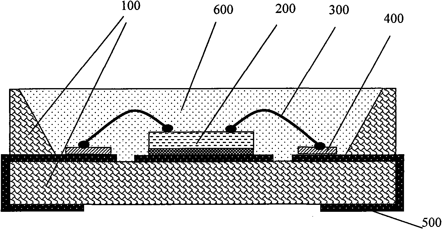
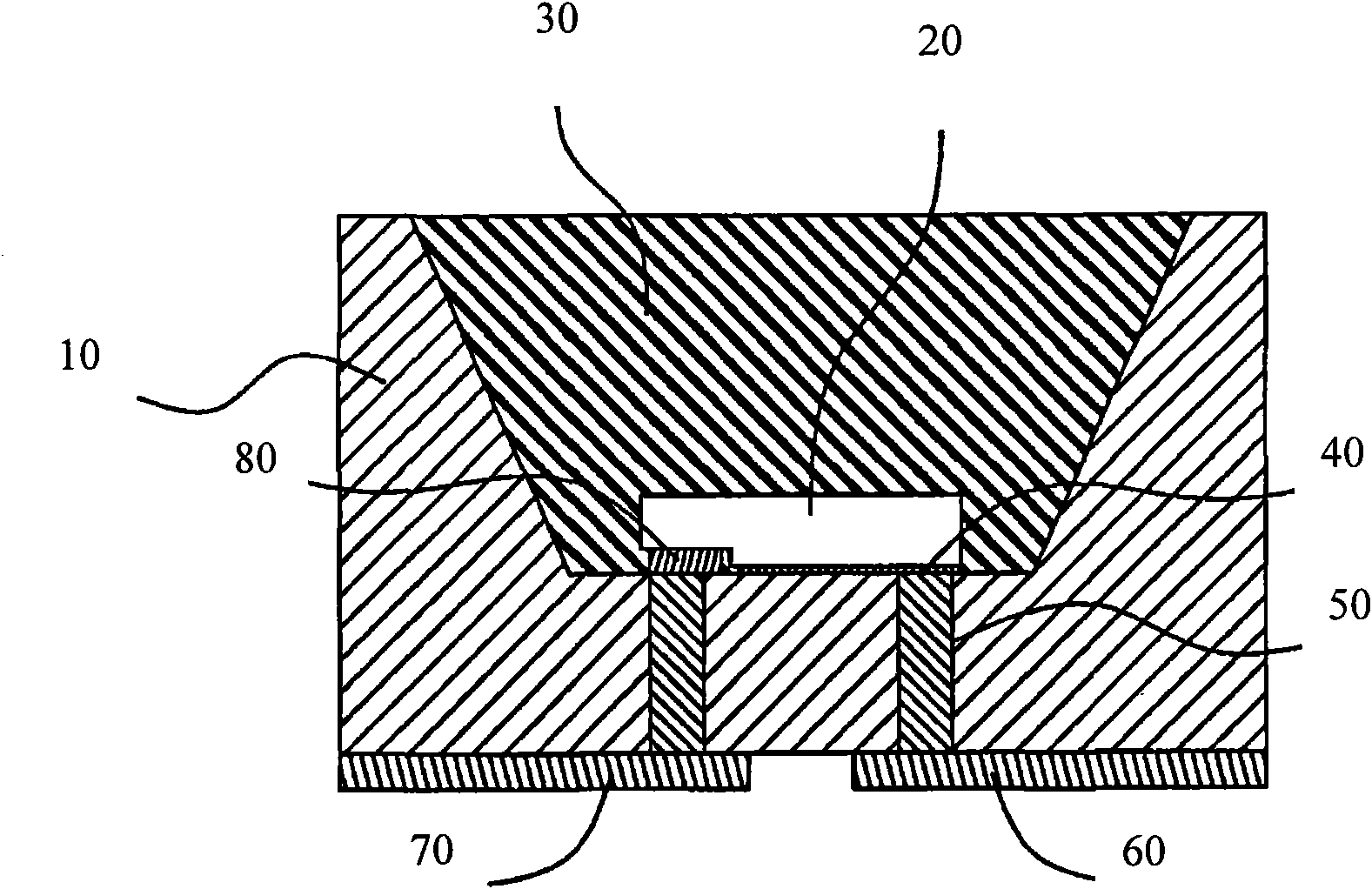
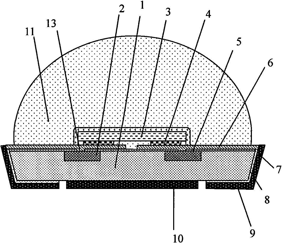
[0052] It is specifically realized in the above step S2. An electrostatic protection circuit 2 and a metal electrode layer 6 are formed on a silicon substrate 1 . For the top view and equivalent circuit diagram of the specific electrostatic protection circuit, please refer to Figure 12 , the circuit is connected in parallel with the two electrodes of the LED chip. The production process is as follows: select a P-type doped silicon substrate 1 with a certain resistivity, first perform a thermal oxidation process on the surface to form an oxide layer 5, and then open a window for the doping position by photolithography etching, and use ion implantation or The diffusion process forms an N-type heavily doped region 2 at the window position, and the doping concentration and depth are determined according to the required PN junction reverse breakdo...

Embodiment 2

[0054] The method for integrating another electrostatic protection circuit on the silicon substrate 1 will be described in detail below.

[0055] It is specifically realized in the above step S2. An electrostatic protection circuit 2 and a metal electrode layer 6 are formed on a silicon substrate 1 . For the top view and equivalent circuit diagram of the specific electrostatic protection circuit, please refer to Figure 13 , the circuit is connected in parallel with the two electrodes of the LED chip. Select an N-type doped silicon substrate 1 with a certain resistivity, first perform a thermal oxidation process on the surface to form an oxide layer 5, and then open a window where the doping position needs to be etched by photolithography, and use ion implantation or diffusion process at the window position Form a P-type heavily doped region 2, the doping concentration and depth are determined according to the required PN junction reverse breakdown voltage; while doping, the...


PUM


Abstract

The invention relates to an LED surface mounting structure for a silicon substrate integrated with functional circuits, which comprises the silicon substrate and an LED chip. The upper surface of the silicon substrate has a planar groove-free structure; an oxidation layer cover the upper surface of the silicon substrate; a metal electrode layer is arranged on the upper surface of the oxidation layer; the upper surface of the metal electrode layer is provided with metal salient points; the LED chip is inversely arranged on the silicon substrate; the lower surface of the silicon substrate is provided with two conductive metal pads which are electrically connected with the metal electrode layer on the upper surface of the silicon substrate through metal leads arranged on the side wall of the silicon substrate; a heat conducting metal pad is arranged on the lower surface of the silicon substrate corresponding to the underside of the LED chip; and the upper surface of the silicon substrate is integrated with peripheral functional circuits required by the LED. The structure has the advantages of good radiating effect and small volume, LED driving and protecting functional circuits are directly integrated in the silicon substrate, wafer-scale industrial packaging is realized and the packaging and lamp cost is reduced.

Description

technical field [0001] The invention belongs to the field of manufacturing light-emitting devices, and relates to an LED packaging structure based on a silicon substrate and a packaging method thereof Background technique [0002] Light-emitting diode (LED) light sources have the advantages of high efficiency, long life, and no harmful substances such as Hg. With the rapid development of LED technology, the brightness and lifespan of LEDs have been greatly improved, making the application of LEDs more and more extensive. From outdoor lighting such as street lamps to indoor lighting such as decorative lamps, they are all used or replaced one after another. into LED as light source. [0003] LED surface mount type (SMD) packaging structure has become the main packaging form due to its advantages of convenient application and small size. see figure 1 , which is a commonly used LED surface mount structure in the prior art, including a package holder 100 and an LED chip 200 mo...

Claims


Application Information

Patent Timeline
Patent Type & Authority Applications(China)
IPC IPC(8): H01L33/48H01L33/62
CPCH01L2924/09701H01L33/62H01L2224/48091H01L2924/10253H01L33/54H01L2224/73265H01L2224/48464H01L2224/48227H01L2224/32225H01L2224/45144H01L33/64H01L33/486H01L24/73H01L2924/14H01L2924/00014H01L2924/00H01L2924/00012
Inventor 曾照明肖国伟陈海英周玉刚侯宇
Owner APT ELECTRONICS
Why Eureka
Try Eureka