
Variable gain low-noise driving amplifier

A drive amplifier with low gain technology, applied in differential amplifiers, DC-coupled DC amplifiers, etc., can solve problems such as difficult to meet performance requirements, high substrate loss, low breakdown voltage, etc., and achieve good overall performance of noise and sensitivity , good input and output matching, small noise figure effect

Inactive Publication Date: 2011-01-12
EAST CHINA NORMAL UNIV
View PDF3 Cites 13 Cited by
  • Summary
  • Abstract
  • Description
  • Claims
  • Application Information

AI Technical Summary

Problems solved by technology

However, the monolithic integrated variable gain low noise drive amplifier using CMOS technology is affected by the lower breakdown voltage of the device, larger parasitic noise, smaller current drive capability and higher substrate loss, and the performance is difficult to achieve. Require

Method used

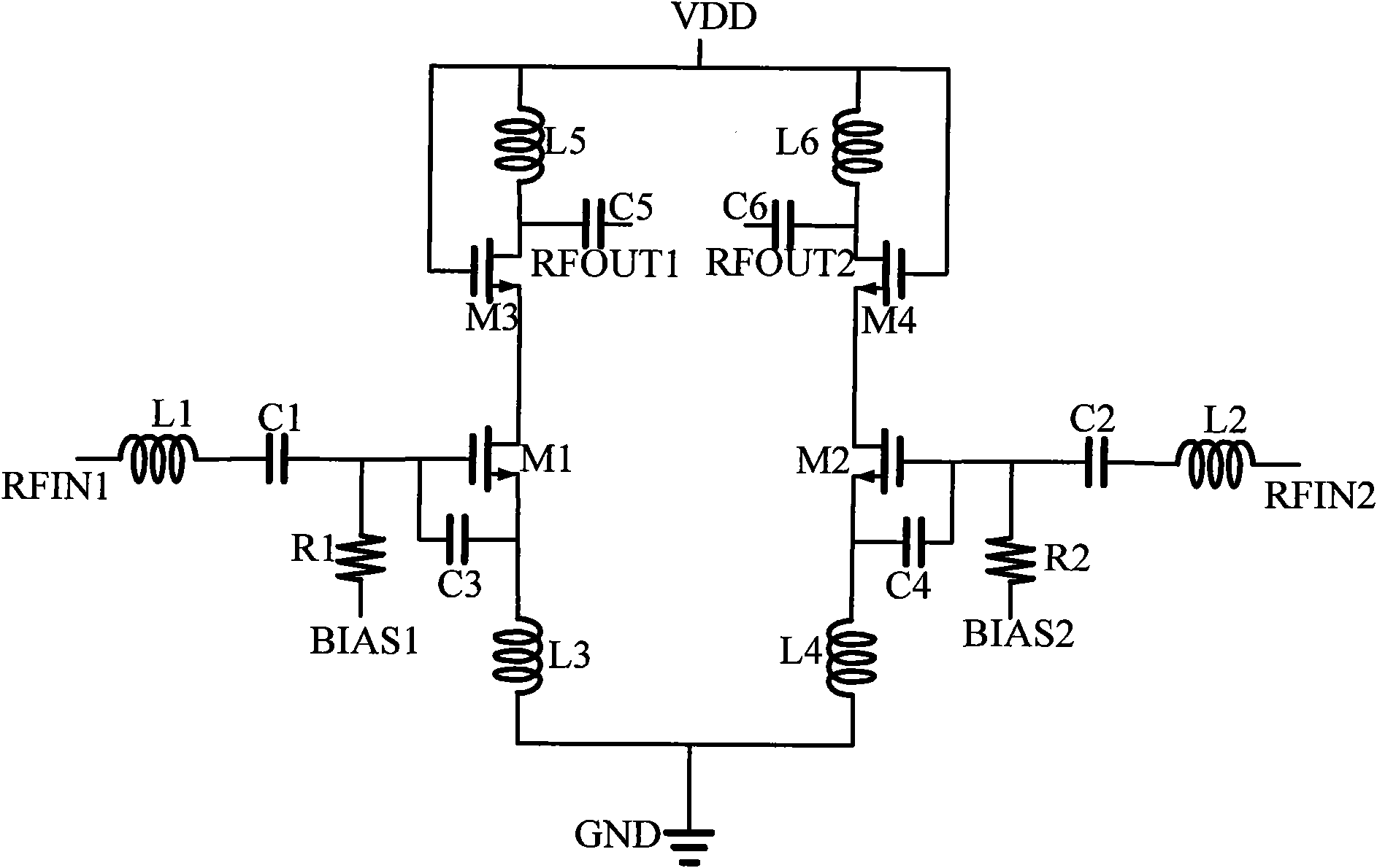
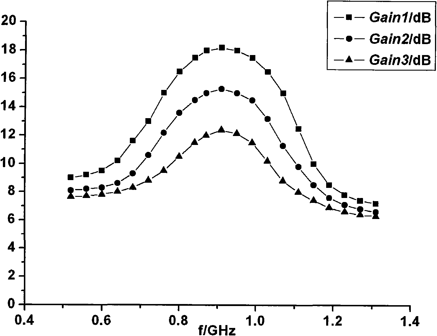

Image

  • Variable gain low-noise driving amplifier
  • Variable gain low-noise driving amplifier
  • Variable gain low-noise driving amplifier

Examples


Embodiment Construction

[0021] Describe the working process of the present invention in detail below.

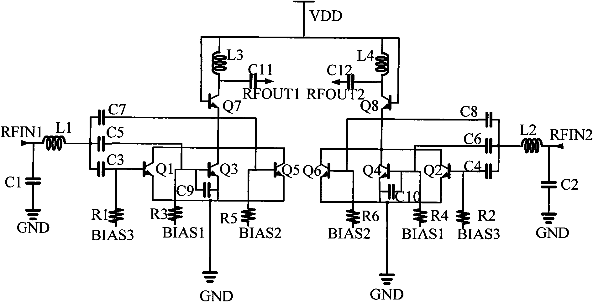
[0022] refer to figure 2, the present invention receives the radio frequency signal from the mixer, outputs it to the power amplifier after being amplified, and then transmits it through the antenna. The power supply voltage VDD is 1.8V, BIAS1 terminal, BIAS2 terminal and BIAS3 terminal are biased at 800mV, and the transistors Q1, Q2, Q3, Q4, Q5, and Q6 are respectively biased at the boundaries of the amplification region and the saturation region by adjusting the bias resistors reasonably. Higher transconductance and lower noise figure are obtained. The fully differential circuit structure is conducive to circuit stability and better overall performance. The RF differential input signal is differentially input through the RFIN1 terminal and RFIN2 terminal, and is differentially output through the RFOUT1 terminal and RFOUT2 terminal. The invention adopts a classic cascode structure, which can o...


PUM


Abstract

The invention discloses a variable gain low-noise driving amplifier. The amplifier has a fully differential cascode structure, wherein a common gate consists of three side-by-side silicon germanide bipolar transistors; the central silicon germanide bipolar transistor adopts parallel capacitive feedback, a reasonable input / output matching circuit is adopted, a high variable gain is provided for a circuit, and the noise coefficient is reduced; a cascade circuit provides a high variable gain and increases the reverse isolation of the circuit at the same time; and a common source amplifying circuit further improves the gain of the circuit. By controlling the selection of an external bias, the variable gain with a 3dB step length is obtained. The variable gain low-noise driving amplifier has the characteristics of high variable gain, low noise and low power consumption.

Description

technical field [0001] The invention belongs to the technical field of radio frequency integrated circuit design, and relates to a silicon germanium bipolar-complementary metal oxide semiconductor (SiGe BiCMOS) radio frequency integrated circuit, specifically a SiGe BiCMOS process variable technology applied to the 860-960MHz frequency band gain low noise driver amplifier. Background technique [0002] In recent years, with the rapid development of radio frequency integrated circuit technology, many wireless communication products are used in daily life, and the requirements of low cost and portability put forward higher standards for the design of these wireless communication products. The low-noise driver amplifier is located at the front end of the radio frequency, receiving the signal from the mixer and then sending it to the power amplifier. Since the conversion gain of the mixer is not high, and the power amplifier needs a large input signal, a low-noise driver amplifi...

Claims


Application Information

Patent Timeline
Patent Type & Authority Applications(China)
IPC IPC(8): H03F3/45
Inventor 刘盛富陈磊赖宗声张伟华林张书霖苏杰阮颖
Owner EAST CHINA NORMAL UNIV
Learn More