Method for preparing nanometer channel with molybdate nanowires
A technology of nano-channel and trimolybdate, which is applied in the direction of nano-structure manufacturing, nano-technology, nano-technology, etc., can solve the problem that it is difficult to change the cross-sectional shape of the channel
- Summary
- Abstract
- Description
- Claims
- Application Information
AI Technical Summary
Problems solved by technology
Method used
Image
Examples
Embodiment 1
[0021] In this embodiment, the following steps are used to prepare nanochannels:
[0022] 1. Prepare pure and uniform K 2 Mo 3 o 10 ·3H 2 O nanowire crystals. The specific preparation method can adopt the method proposed by the patent No. ZL200810119770.2, titled "A Preparation Method of Potassium Trimolybdate Trihydrate Nanowire". The radial cross section of the nanowires prepared by this method is circular.
[0023] 2. Disperse the prepared nanowires on the silicon substrate. During the dispersion process, the nanowires should be dispersed as thoroughly as possible, and the phenomenon of overlapping or clustering should be eliminated as much as possible. The dispersion density of nanowires on the silicon substrate is within 100 μm 2 There are about 5. This process can also be carried out with nanoprobes, by which the nanowires are placed in predetermined positions.
[0024] 3. Coat photoresist on the silicon substrate and carry out photoetching according to the desig...
Embodiment 2
[0028] In this embodiment, the following steps are used to prepare nanochannels:
[0029] 1. Prepare pure and uniform NaNH 4 Mo 3 o 10 ·H 2 O nanowire crystals.
[0030] 2. Disperse the prepared nanowires on the silicon substrate. During the dispersion process, the nanowires are completely dispersed without overlapping or clustering. per 100μm 2 There are about 5 nanowires on the silicon substrate. This process can also be used to place nanowires at predetermined locations via nanoprobes.
[0031] 3. A chromium thin film is grown on the silicon substrate, and the thickness of the chromium thin film is about 200nm.
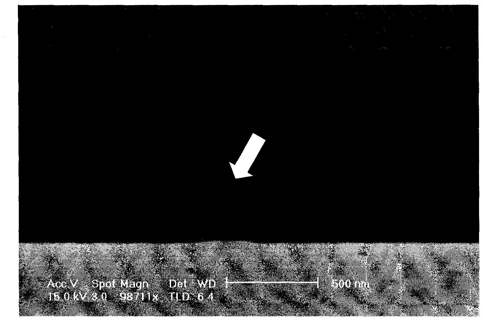
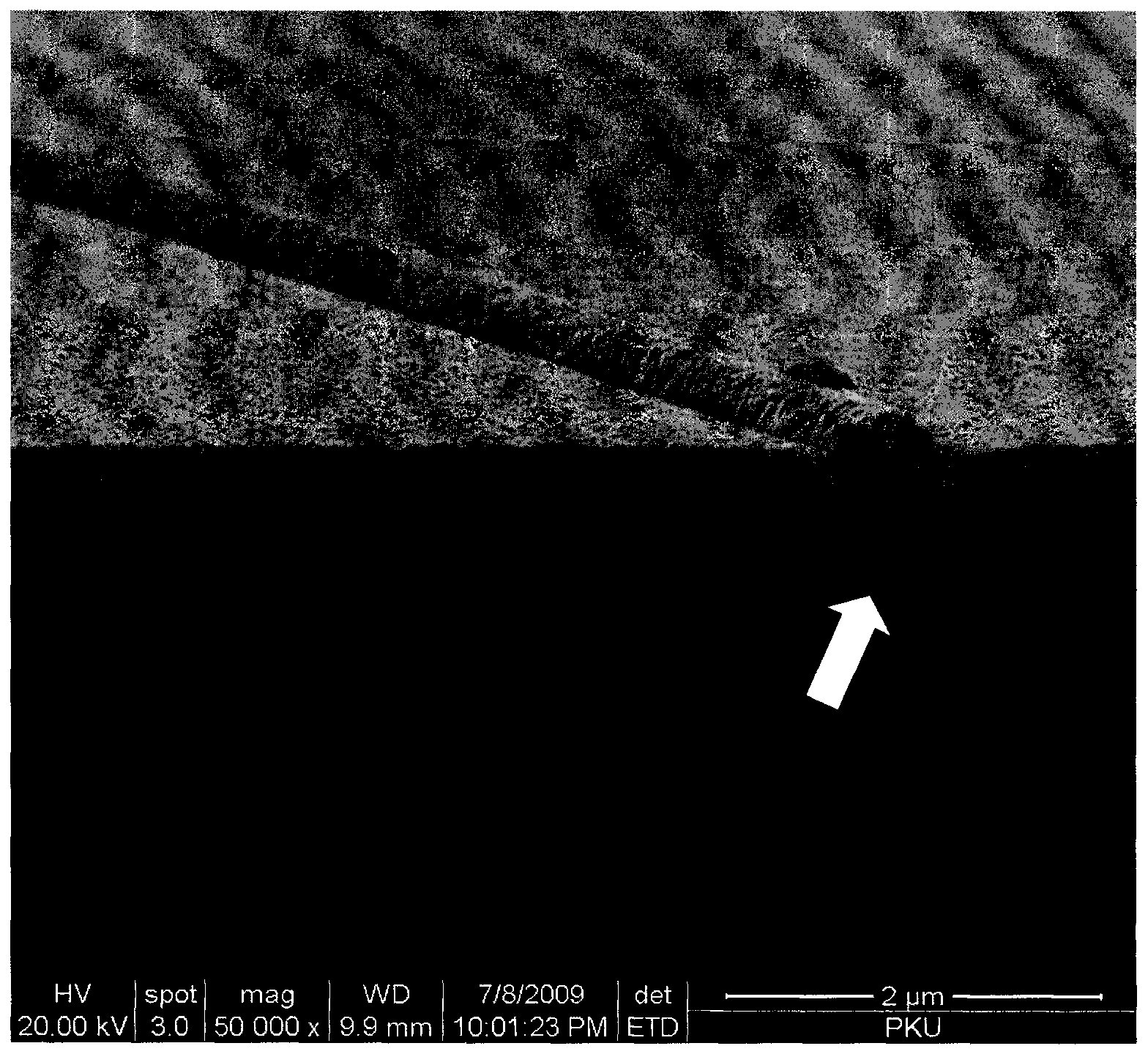
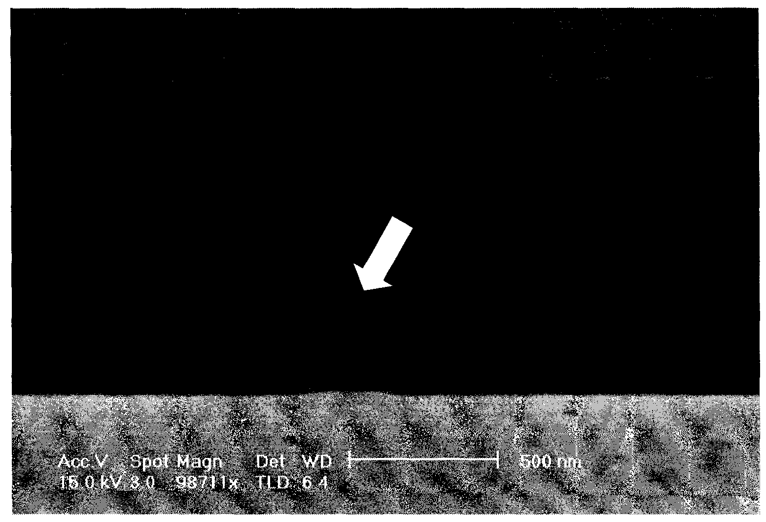
[0032] 4. Dissolve the nanowires as the sacrificial material with deionized water, and the grooves left are nanochannels. The nanochannels were made against the silicon substrate on one side, and the other sides of the channel were chromium. Such as figure 2 shown.
[0033] The nanochannels prepared by this method are basically all hexagonal in cross-se...
PUM
| Property | Measurement | Unit |
|---|---|---|
| thickness | aaaaa | aaaaa |
Abstract
Description
Claims
Application Information
 - Generate Ideas
- Intellectual Property
- Life Sciences
- Materials
- Tech Scout
- Unparalleled Data Quality
- Higher Quality Content
- 60% Fewer Hallucinations
Browse by: Latest US Patents, China's latest patents, Technical Efficacy Thesaurus, Application Domain, Technology Topic, Popular Technical Reports.
© 2025 PatSnap. All rights reserved.Legal|Privacy policy|Modern Slavery Act Transparency Statement|Sitemap|About US| Contact US: help@patsnap.com


