Acoustic surface wave icing sensor capable of accessing wirelessly
An icing sensor and surface acoustic wave technology, applied in radio wave measurement systems, using ultrasonic/sonic/infrasonic waves, and using sonic/ultrasonic/infrasonic waves to analyze solids, etc., can solve the problem that icing sensors cannot measure wirelessly, and achieve application Convenience, low price, high sensitivity effect
- Summary
- Abstract
- Description
- Claims
- Application Information
AI Technical Summary
Problems solved by technology
Method used
Image
Examples
Embodiment 1
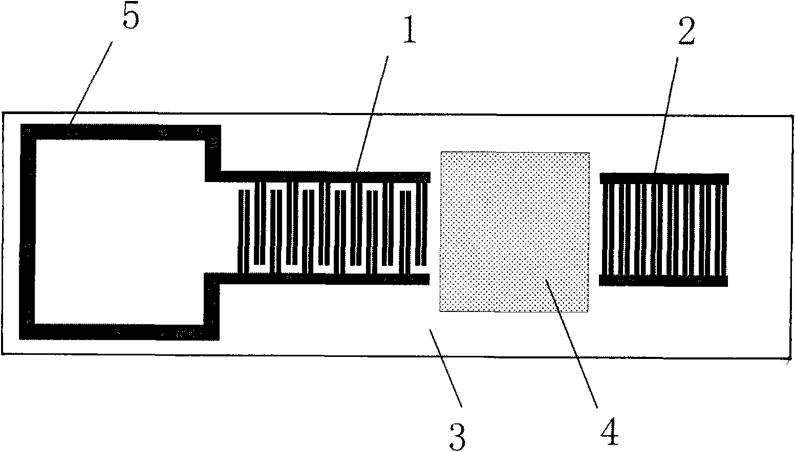
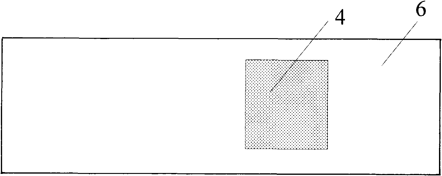
[0026] Such as figure 1 , figure 2 As shown, the surface acoustic wave icing sensor mainly includes: a piezoelectric substrate 3 , an interdigital transducer 1 , a reflection grid 2 , an antenna 5 , a photoresist waveguide layer 4 and an encapsulation layer 6 . Through the processes of film washing, film coating, glue removal, photolithography, cleaning, etc., the dipole antenna 5, interdigital transducer 1 and reflection grid 2 are attached to the piezoelectric substrate 3 of ST900X quartz, and the center frequency is 433-500MHZ , the insertion loss of no-load passing through the antenna 5 is 15 ~ 25dB, and the SU8 2050 photoresist waveguide layer 4 is attached to the piezoelectric substrate 3 through processes such as glue rejection, pre-baking, photolithography, and post-baking, and is located at the interdigital Between the transducer 1 and the reflection grid 2, the thickness is 2-3 μm. The interdigital transducer 1, reflection grid 2, antenna 5, and piezoelectric subs...
Embodiment 2
[0028] Concrete craft making and principle are as embodiment 1, as Figure 4 , Figure 5 shown. The differences are: (1) During the process of attaching the SU82050 photoresist waveguide layer 4 to the piezoelectric substrate 3, the area of the photoresist waveguide layer 4 covers the IDT 1 and the reflective grating 2; (2) A part of the SU 82050 photoresist waveguide layer 4 is exposed during packaging, and it is used as a sensitive area to effectively protect the IDT 1 and the reflection grid 2 . The encapsulation layer 6 has no effect on the emission and reception of electromagnetic waves, but the encapsulation layer 6 can effectively protect the cross-value transducer and the reflection grid, so that the sensor can be applied in a relatively complex natural environment. The structure after encapsulation is as follows Figure 6 shown.
Embodiment 3
[0030] The specific embodiment is as in Example 1, and the structure is as Figure 4 , Figure 5shown. The differences are: (1) PMMA glue is used as the waveguide layer, and the PMMA glue is attached to the piezoelectric substrate 3 to cover the interdigital transducer 1 and the reflection grid 2; (2) the piezoelectric substrate 3 uses 360 lithium tantalate.
PUM
 Abstract
Description
Claims
Application Information
 - Generate Ideas
- Intellectual Property
- Life Sciences
- Materials
- Tech Scout
- Unparalleled Data Quality
- Higher Quality Content
- 60% Fewer Hallucinations
Browse by: Latest US Patents, China's latest patents, Technical Efficacy Thesaurus, Application Domain, Technology Topic, Popular Technical Reports.
© 2025 PatSnap. All rights reserved.Legal|Privacy policy|Modern Slavery Act Transparency Statement|Sitemap|About US| Contact US: help@patsnap.com


