Plasma radiation source with axial magnetic field

A radiation source, magnetic field technology, applied in the field of device manufacturing, can solve problems such as damage to reflective elements

Inactive Publication Date: 2009-12-16
ASML NETHERLANDS BV
View PDF1 Cites 2 Cited by
  • Summary
  • Abstract
  • Description
  • Claims
  • Application Information

AI Technical Summary

Problems solved by technology

Unfortunately, these fast ions can cause damage to reflective elements in lithographic equipment

Method used


Image

  • Plasma radiation source with axial magnetic field
  • Plasma radiation source with axial magnetic field
  • Plasma radiation source with axial magnetic field

Examples


Embodiment Construction

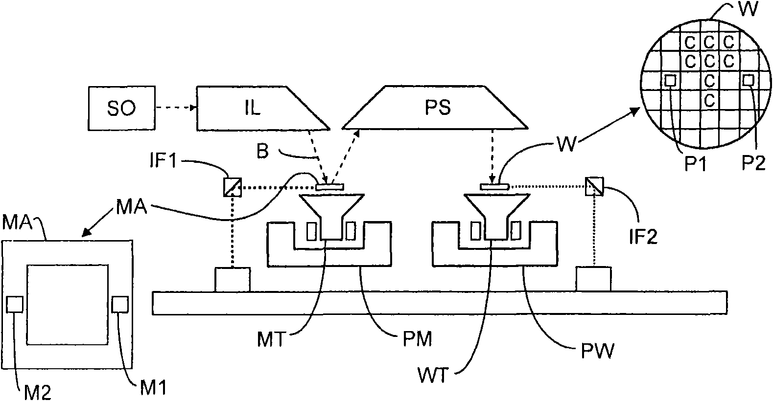
[0023] figure 1 A lithographic apparatus according to an embodiment of the invention is schematically shown. The lithography equipment includes:

[0024] - an illumination system (illuminator) IL configured to condition a radiation beam B (eg, ultraviolet (UV) radiation or extreme ultraviolet (EUV) radiation);

[0025] - a support structure (eg mask table) MT configured to support the patterning device (eg mask) MA and connected to first positioning means PM configured to precisely position the patterning device according to determined parameters;

[0026] - a substrate table (e.g. a wafer table) WT configured to hold a substrate (e.g. a resist-coated wafer) W and associated with a second positioning device configured to precisely position the substrate according to determined parameters PW connected; and

[0027] - A projection system (eg a reflective projection system) PS configured to project the pattern imparted to the radiation beam B by the patterning device MA onto a...


PUM


Abstract

A patterned beam of radiation is projected onto a substrate. A reflective optical element is used to help form the radiation beam from radiation emitted from a plasma region of a plasma source. In the plasma source, a plasma current is generated in the plasma region. To reduce damage to the reflective optical element, a magnetic field is applied in the plasma region with at least a component directed along a direction of the plasma current. This axial magnetic field helps limit the collapse of the Z-pinch region of the plasma. By limiting the collapse, the number of fast ions emitted may be reduced.

Description

technical field [0001] The invention relates to a plasma radiation source, an apparatus for forming a radiation beam using a plasma radiation source (in an embodiment the apparatus is a lithographic apparatus), a method for forming plasma radiation and A device manufacturing method. Background technique [0002] A lithographic apparatus is a machine that applies a desired pattern to a substrate, usually a target portion of the substrate. For example, lithographic equipment may be used in the manufacture of integrated circuits (ICs). In this case, a patterning device, alternatively referred to as a mask or reticle, may be used to generate the circuit pattern to be formed on the individual layers of the IC. The pattern can be transferred onto a target portion (eg, comprising a portion, one or more dies) on a substrate (eg, a silicon wafer). Typically, the pattern is transferred by imaging the pattern onto a layer of radiation sensitive material (resist) provided on the subs...

Claims


Application Information

Patent Timeline
Patent Type & Authority Applications(China)
IPC IPC(8): H05G2/00G03F7/20
CPCB82Y10/00G03F7/70033G03F7/70916H05G2/003H05G2/005H05G2/00G03F7/20
Inventor V·V·伊凡诺夫V·Y·班尼恩K·N·柯什烈夫
Owner ASML NETHERLANDS BV
Why Eureka
Try Eureka