Digital micro-droplet drive with deep submicron pore structure and manufacturing method thereof
A deep submicron and manufacturing method technology, applied in the direction of microstructure technology, microstructure devices, chemical instruments and methods, etc., can solve the problems of difficult processing of micro-convex structures, increase in the thickness of the dielectric layer, and reduce the driving voltage, etc., so as to facilitate mass production The effect of making, reducing the driving voltage, and reducing the resistance
- Summary
- Abstract
- Description
- Claims
- Application Information
AI Technical Summary
Problems solved by technology
Method used
Image

Examples
Embodiment 1
[0020] Example 1: Micro-droplet driver with deep submicron pore structure of unipolar plate structure.
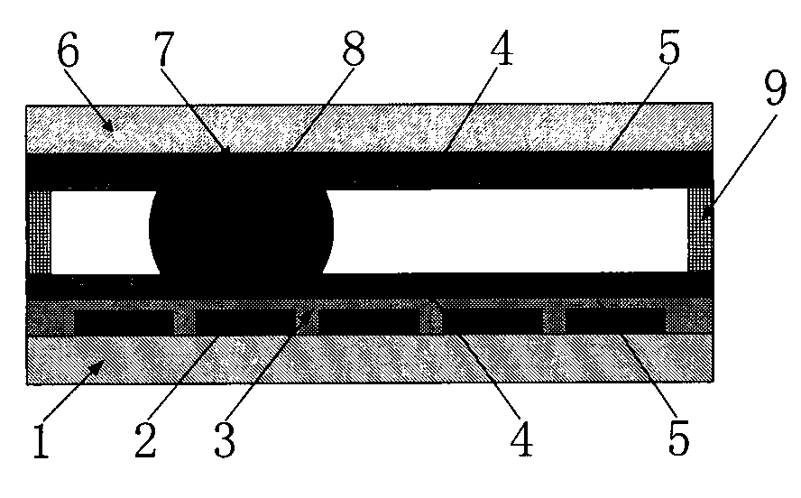
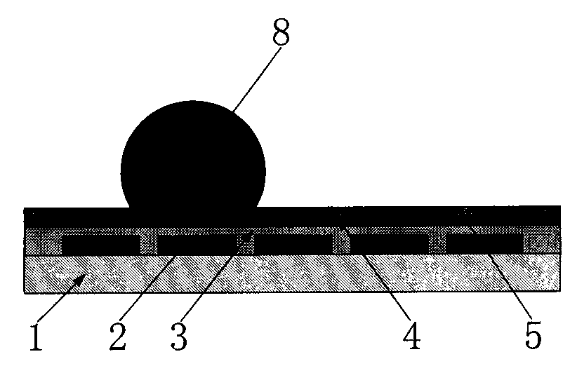
[0021] This embodiment adopts the structure shown in Figure 1(b), in which a layer of thermally oxidized SiO 2 The Si sheet is used as the substrate material, TiW / Au is used as the driving electrode, the SiN thin film of PECVD is used as the dielectric layer, and the deep submicron pore structure and low surface energy fluorocarbon polymer composite film prepared by Al anodic oxidation are used as the hydrophobic film layer. . The electrodes are 1mm×1mm square, the distance between the electrodes is 30μm, the electrodes are arranged regularly, and each electrode can be controlled individually. The chips operate directly in an air atmosphere.
[0022] The specific production process is as follows:
[0023] (1) Use ordinary single-polishing (100) silicon wafers with a thickness of 450 μm, clean and oxidize 1 μm.
[0024] (2) Sputter TiW with a thickness of 50nm and gold w...
Embodiment 2
[0030] Example 2: Micro-droplet driver with deep submicron pore structure of bipolar plate structure.
[0031] This embodiment adopts the structure shown in FIG. 1( a ), and the manufacturing process and flow of the lower plate are exactly the same as those in Embodiment 1. The upper plate uses glass (Pyrex7740) as the substrate, transparent indium tin oxide (ITO) as the reference electrode layer, the thickness of the reference electrode layer is between 200nm and 1μm, and the deep submicron pore structure prepared by Al anodic oxidation And low surface energy fluorocarbon polymer composite membrane as the hydrophobic membrane layer. The support structure can be made of photoresist or double-sided tape, and the upper and lower plates can be assembled after being aligned through the support structure.
[0032]The manufacturing process of the upper plate and the supporting structure is as follows: first, a 500nm-thick ITO layer is prepared on the Pyrex7740 glass substrate by va...
PUM
| Property | Measurement | Unit |
|---|---|---|
| thickness | aaaaa | aaaaa |
| thickness | aaaaa | aaaaa |
| thickness | aaaaa | aaaaa |
Abstract
Description
Claims
Application Information
 - R&D
- Intellectual Property
- Life Sciences
- Materials
- Tech Scout
- Unparalleled Data Quality
- Higher Quality Content
- 60% Fewer Hallucinations
Browse by: Latest US Patents, China's latest patents, Technical Efficacy Thesaurus, Application Domain, Technology Topic, Popular Technical Reports.
© 2025 PatSnap. All rights reserved.Legal|Privacy policy|Modern Slavery Act Transparency Statement|Sitemap|About US| Contact US: help@patsnap.com