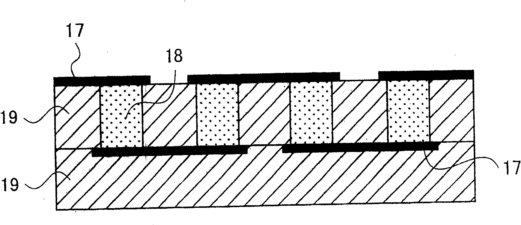
Adhesion assisting agent-bearing metal foil, printed wiring board using the same and manufacturing method thereof
A printed circuit board and auxiliary agent technology, applied in the field of metal foil, can solve the problems of good high-frequency characteristics, and achieve the effects of good high-frequency characteristics, high reliability, and improved adhesion
- Summary
- Abstract
- Description
- Claims
- Application Information
AI Technical Summary
Problems solved by technology
Method used
Image
Examples
Embodiment 1
[0201] Metal foil A described below was produced.
[0202] (metal foil A)
[0203] Under the following conditions, the glossy surface of electrolytic copper foil (carrier copper foil) with a width of 510 mm and a thickness of 35 μm was continuously plated with chrome to form a 1.0 mg / dm 2 Thick chrome plating (stripping layer). The surface roughness Rz after the chromium plating layer was formed was 0.5 μm. The surface roughness was measured according to JIS-B-0601.
[0204] Chrome Plating Condition
[0205] Solution composition: chromium trioxide 250g / L, sulfuric acid 2.5g / L
[0206] Bath temperature: 25°C
[0207] Anode: lead
[0208] Current density: 20A / dm 2
[0209] Next, copper electroplating with a thickness of 2.0 μm was performed under the following gloss plating conditions. The surface roughness of the metal foil after copper electroplating is Rz=0.6 μm.
[0210] Sulfuric acid copper plating conditions
[0211] Solution composition: copper sulfate pentahydra...
Embodiment 2
[0279] When making resin composition A in embodiment 1, the consumption of the novolac type epoxy resin (NC3000S-H) with biphenyl structure is changed from 80 parts by weight to 82.8 parts by weight, and the cresol novolac containing triazine ring The amount of type phenolic resin (Feenolite EXB-9289) was changed from 9 parts by weight to 12.2 parts by weight. Others are all the same as embodiment 1 to make a printed circuit board.
Embodiment 3
[0281] A printed wiring board was produced in the same manner as in Example 1 except that the thickness of the resin composition A was changed from 2.0 μm to 5 μm when producing the metal foil B in Example 1.
PUM
| Property | Measurement | Unit |
|---|---|---|
| Surface roughness | aaaaa | aaaaa |
| Current density | aaaaa | aaaaa |
| Surface roughness | aaaaa | aaaaa |
Abstract
Description
Claims
Application Information
 - R&D
- Intellectual Property
- Life Sciences
- Materials
- Tech Scout
- Unparalleled Data Quality
- Higher Quality Content
- 60% Fewer Hallucinations
Browse by: Latest US Patents, China's latest patents, Technical Efficacy Thesaurus, Application Domain, Technology Topic, Popular Technical Reports.
© 2025 PatSnap. All rights reserved.Legal|Privacy policy|Modern Slavery Act Transparency Statement|Sitemap|About US| Contact US: help@patsnap.com


