
Method for manufacturing patterned magnetic recording medium

A technology for magnetic recording media and manufacturing methods, applied in the direction of disc carrier manufacturing, different record carrier forms, and only a part of the coating supported by a magnetic layer, which can solve the problems of magnetic head damage, magnetic characteristic changes, and magnetic layer deterioration. , to achieve the effects of deterioration suppression, stable detection, and prevention of re-pollution

Inactive Publication Date: 2009-09-02
FUJI ELECTRIC CO LTD +1
View PDF4 Cites 2 Cited by
  • Summary
  • Abstract
  • Description
  • Claims
  • Application Information

AI Technical Summary

Problems solved by technology

Heat treatment may also cause deterioration of the magnetic layer, change (decrease) of magnetic properties
[0013] In addition, when the resist film remains on the magnetic layer instead of completely peeling off the resist film on the magnetic layer, it is difficult for the magnetic head to float stably.
As a result, the magnetic signal of the magnetic recording medium cannot be detected stably.
Depending on the situation, the head itself may be destroyed by hitting the remaining resist

Method used


Image

  • Method for manufacturing patterned magnetic recording medium
  • Method for manufacturing patterned magnetic recording medium
  • Method for manufacturing patterned magnetic recording medium

Examples


Embodiment 1

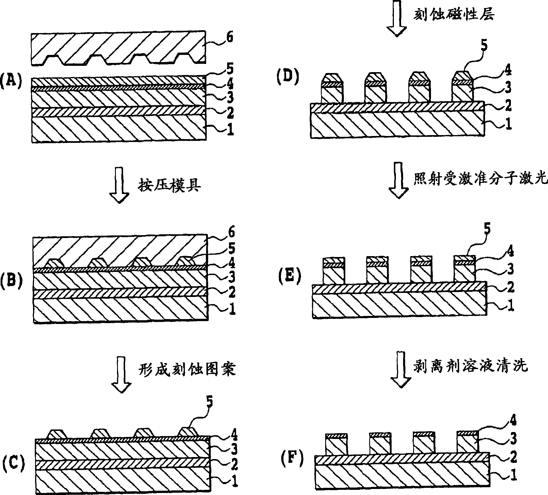
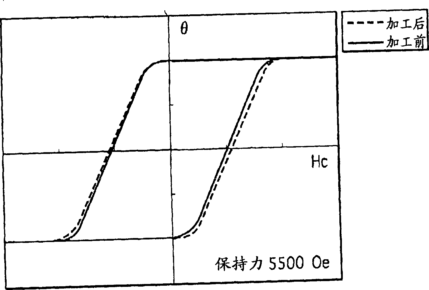
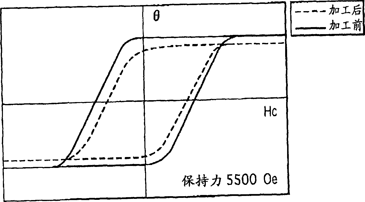
[0070] On a 2.5-inch glass substrate 1, a base layer 2 with a thickness of 30nm and a layer of CoCrPtSiO with a thickness of 20nm are laminated. 2 The magnetic layer 3 and the carbon first protective layer 4 with a thickness of 3nm were used to produce a magnetic recording medium. The recording medium has figure 2 Magnetic properties shown in solid lines. Then, a thermosetting resist mr-I-8010E (trade name, manufactured by Micro Resist Technology GmbH) with a thickness of 100 nm was applied on the first protective layer 4 by spin coating to form a resist. Etch coating 5.

[0071] A nickel mold 6 heated to 180° C., having a track-like pattern with a width of 80 nm and a depth of 60 nm, was pressed against the formed resist film 5 for 30 seconds using a pressing device at a pressure of 100 MPa (1000 bar). After 10 minutes, the resist is cured to form an etching pattern on the resist film 5 .

[0072] using O 2 After the resist film 5 remaining at the bottom of the etched pa...

Embodiment 2

[0078] In addition to changing the irradiation atmosphere of the excimer VUV laser in Example 1 to a nitrogen atmosphere with a pressure of 0.6KPa (60mbar), and changing the irradiation distance to 2.7mm, the same conditions as in Example 1 were used to carry out anti-corrosion. The etchant film 5 is peeled off to manufacture a patterned magnetic recording medium.

[0079] By FT-IR analysis after the DMF solution cleaning treatment, it was confirmed that the resist on the first protective layer 4 was completely removed. In addition, as in Example 1, the magnetic properties of the magnetic recording medium measured by Kerr remained unchanged before and after patterning.


PUM

PropertyMeasurementUnit
widthaaaaaaaaaa
depthaaaaaaaaaa

Abstract

The invention provides a method for manufacturing a patterned magnetic recording medium including a step of completely removing an etching resist on a magnetic layer 3, which is used for etching the magnetic layer 3, without deteriorating magnetic characteristics of the magnetic layer 3. The step of removing the etching resist used for etching the magnetic layer 3 includes the steps of irradiating the etching resist on the magnetic layer 3 or the first protective layer 4 with an excimer VUV laser under a reduced pressure and immersing the resist coating 5 remaining on the magnetic layer 3 or the first protective layer 4 into a resist removing agent solution to wash off the resist coating 5.

Description

technical field [0001] The present invention relates to a method for manufacturing a patterned magnetic recording medium, and more specifically, to an improvement in a method for removing a resist used when processing a magnetic layer into a track-like and / or dot-like pattern. Background technique [0002] As a next-generation magnetic recording medium, a patterned magnetic recording medium in which a magnetic layer is processed into a track-like and / or dot-like pattern and information recording regions are respectively defined on the patterned magnetic layer is expected. [0003] These patterned magnetic recording media, as disclosed in Japanese Patent Application Laid-Open No. 2003-203301 and Japanese Patent Laid-Open No. 2003-123201, in addition to recording normal information in the demarcated information recording area, can also Inherent information of the recording medium, such as manager information of the information, operation information, etc., is recorded. Theref...

Claims


Application Information

Patent Timeline
Patent Type & Authority Applications(China)
IPC IPC(8): G11B5/855G11B5/74
CPCG11B5/855G11B5/84
Inventor 梶原里美庄子习一水野润篠原秀敏
Owner FUJI ELECTRIC CO LTD
Learn More