Conductive film forming method, thin film transistor, panel with thin film transistor and thin film transistor manufacturing method

A technology of thin film transistors and conductive films, applied in semiconductor/solid-state device manufacturing, transistors, electric solid-state devices, etc., can solve the problems of resistive hillock patience and low adhesion, and achieve high adhesion and contact The effect of low resistance and low resistance

Inactive Publication Date: 2009-08-19
ULVAC INC
View PDF2 Cites 7 Cited by
  • Summary
  • Abstract
  • Description
  • Claims
  • Application Information

AI Technical Summary

Problems solved by technology

[0007] As a patent related to a metal wiring film for electronic components with Cu as the main component, a technique characterized by adding elements such as Mo to Cu is known (Japanese Patent Laid-Open No. In the step of film formation, the technology characterized by introduction of nitrogen or oxygen (Japanese Patent Laid-Open No. 10-12151), but both have problems in adhesion, low resistance, and tolerance to hillocks

Method used


Image

  • Conductive film forming method, thin film transistor, panel with thin film transistor and thin film transistor manufacturing method
  • Conductive film forming method, thin film transistor, panel with thin film transistor and thin film transistor manufacturing method
  • Conductive film forming method, thin film transistor, panel with thin film transistor and thin film transistor manufacturing method

Examples


Embodiment

[0086]

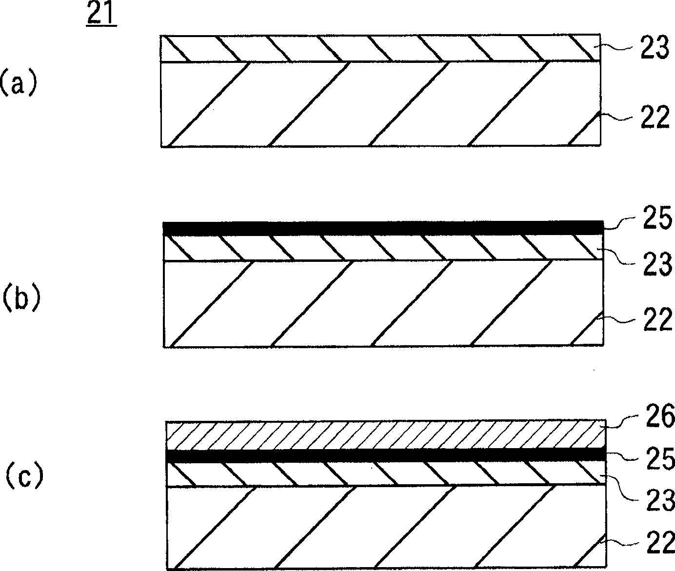
[0087]As the main target 11 , a copper (purity: 99.9 at % or more) target with a diameter of 7 inches was used, and as the sub-target 12 , a target made of Ti was used.

[0088] The conductive film 25 was formed on the surface of the glass substrate by changing the Ti content in the conductive film 25 , the partial pressure of nitrogen gas during film formation, and the heating temperature (post-annealing temperature) during annealing treatment, and 125 kinds of test pieces were produced.

[0089] Further, except that the sub-target 12 was changed to a target made of Zr, the conductive film 25 was formed on the surface of the glass substrate by the same procedure as above, and 125 kinds of test pieces were produced.

[0090] In addition, the film forming conditions of each conductive film 25 are: the target film thickness of the conductive film 25 is 300 nm, the sputtering gas is Ar gas, and the total pressure inside the first film forming chamber 2 is 0.4 Pa. The c...


PUM


Abstract

A conductive film having high adhesiveness and low specific resistance is formed. A target having copper as a main component is sputtered in a vacuum atmosphere into which nitrogen gas is introduced, and a conductive film (25) containing copper as a main component and added metals such as Ti is formed. The conductive film (25) has high adhesiveness to a silicon layer (23) and a substrate (22), and is not easily removed from over the substrate (22). Furthermore, since the conductive film has the low specific resistance and a low contact resistance to a transparent conductive film, its electrical characteristics do not deteriorate even when it is used as an electrode film. The conductive film formed by this invention is specially suitable for barrier films for electrodes for TFTs and semiconductor elements.

Description

technical field [0001] The present invention relates to a metal wiring film suitable for use in electronic components and a sputtering method as a film forming method thereof. Background technique [0002] Conventionally, low-resistance materials such as Al or Cu, or Mo, Cr, or the like have been used for metal wiring films for electronic devices. For example, in a TFT (Thin film transistor) liquid crystal display, as the size of the panel increases, the demand for lower resistance of the wiring electrodes also increases, and the necessity of using Al or Cu as the low-resistance wiring increases. [0003] The Al wiring used in the TFT has the problem of hillock formation in subsequent steps or the diffusion into the Si layer of the base material when the Al wiring is used as the source and drain, and the contact resistance with the transparent electrode containing ITO (indium-tin oxide) deteriorates. In order to avoid these problems, it is necessary to laminate Mo or Cr and...

Claims


Application Information

Patent Timeline
Patent Type & Authority Applications(China)
IPC IPC(8): H01L21/285G02F1/1343G02F1/1368G09F9/00H01L21/28H01L21/3205H01L21/336H01L23/52H01L29/786
CPCH01L21/2855H01L21/76843G02F1/1368C23C14/0036H01L27/1214H01L29/458H01L29/4908H01L27/12H01L23/53238C23C14/185H01L2924/12044G02F2001/136295H01L21/32051H01L27/124H01L2924/0002G02F1/136295H01L2924/00
Inventor 高泽悟武井应树高桥明久浮岛祯之谷典明石桥晓
Owner ULVAC INC
Why Eureka
Try Eureka