Electrode for in-situ electrical measurement for diamond anvil cell and method for producing the same
The invention relates to a technology of diamond counter-anvil and manufacturing method, which is applied to the field of boron-doped diamond film electrodes, and can solve the problems of difficulty in electrode arrangement, measurement failure, electrode deformation, etc., and achieve high chemical and electrochemical stability and improve reliability. , to overcome the effect of corrosion
- Summary
- Abstract
- Description
- Claims
- Application Information
AI Technical Summary
Problems solved by technology
Method used
Image
Examples
Embodiment 1
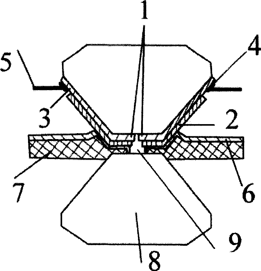
[0021] Example 1 Combined figure 1 and figure 2 The structure of the electrode of the present invention will be described.
[0022] figure 1 and figure 2 Among them, 1 is an electrode, and there are 4 electrodes. The ends of each electrode 1 on the surface of the diamond anvil are square and are located in the sample chamber 9 of the diamond anvil, and the electrode ends 3 on the side of the diamond anvil are connected. Electrode leads 5 with copper wires, electrode 1 of boron-doped diamond film are covered by insulating layer 2 of diamond film except two ends; 2 is diamond insulating layer; 3 is the electrode terminal on the side of diamond anvil; 4 5 is the electrode lead, and the electrode lead 5 is connected to the electrode terminal 3 on the side of the diamond anvil through the silver paste 4; 6 is the aluminum oxide insulating layer; 7 is the T301 steel gasket, and the aluminum oxide insulating layer 6 is placed on the On it; 8 is a diamond anvil, and two diamond ...
Embodiment 2
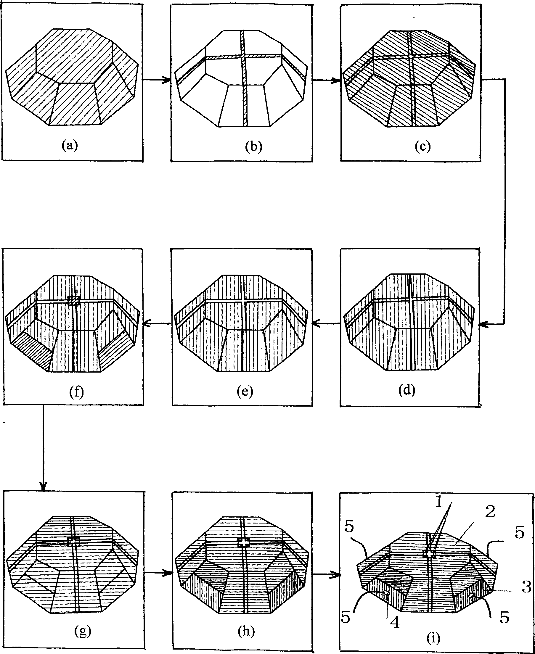
[0024] Example 2 Combined image 3 The process of making the electrode of the present invention is described.
[0025] Step 1: Soak the diamond anvil in a mixture of acetone and alcohol for 20 minutes to remove surface stains, take it out and rinse it with deionized water. After drying, it is placed in a vacuum chamber, and an aluminum oxide film is deposited on the diamond surface by magnetron sputtering. like image 3 (a) shown.
[0026] In the sputtering process, metal aluminum is used as the target material, oxygen and argon with a flow ratio of 30:2.0-3.0 are used as the working gas, the pressure in the vacuum chamber is kept at 0.8-1.2Pa, and the substrate temperature is kept at 200 ℃—300℃.
[0027] The second step: take out the diamond coated with aluminum oxide film, apply a layer of photoresist evenly on its surface, use photolithography technology to carve the crosshair shape on the diamond anvil surface, and then corrode it with corrosive solution (in phosphoric...
Embodiment 3
[0039] Embodiment 3 The manufacturing process of two electrodes on the diamond anvil of the present invention.
[0040] Whole technological process is identical with embodiment 2. It is only in the second step that photolithography is used to make an electrode isolation zone, which passes from one side of the diamond anvil through the sample cavity in the center of the anvil to the opposite side of the diamond anvil; the sixth step is to Two alumina squares were left on the sides of the diamond anvil.
PUM
| Property | Measurement | Unit |
|---|---|---|
| Width | aaaaa | aaaaa |
| Thickness | aaaaa | aaaaa |
Abstract
Description
Claims
Application Information
 - R&D
- Intellectual Property
- Life Sciences
- Materials
- Tech Scout
- Unparalleled Data Quality
- Higher Quality Content
- 60% Fewer Hallucinations
Browse by: Latest US Patents, China's latest patents, Technical Efficacy Thesaurus, Application Domain, Technology Topic, Popular Technical Reports.
© 2025 PatSnap. All rights reserved.Legal|Privacy policy|Modern Slavery Act Transparency Statement|Sitemap|About US| Contact US: help@patsnap.com


