


Quick Research
Generate reliable direction feasibility study reports for your R&D in just a few steps.

Technical Q&A
Discover and master advanced knowledge NOW. Basics, ideas, possibilities, all at once.

Find Solutions
As an expert in R&D theories, this can generate solutions to your technical problems instantly.

Evaluate Feasibility
Analyze your overall solution with one click, know your potential R&D risks in advance.

Monitor Landscape
Get weekly tech updates, stay abreast of the latest tech innovations and key insights.
Test structure and method for detecting disc trap and corrosion caused by CMP
A test structure and test line technology, applied in semiconductor/solid-state device testing/measurement, electrical components, electric solid-state devices, etc., can solve problems such as erosion, copper wire sag, and inability to detect at any time, and achieve accurate test results.
- Summary
- Abstract
- Description
- Claims
- Application Information
AI Technical Summary
Problems solved by technology
Method used
Image

Examples
Embodiment 1
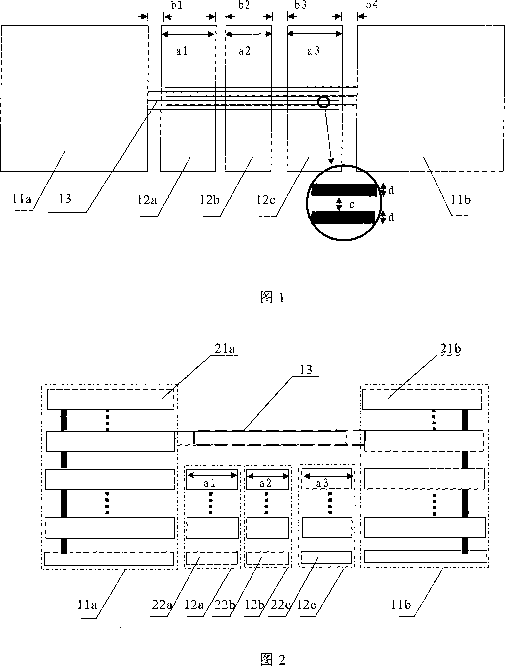
[0039] In this embodiment, a 0.13 μm copper wiring process is used, and this test structure is used to test the copper wiring on the fourth metal layer caused by the dishing of the copper metal area produced by CMP on the metal block on the first metal layer. influence level.
[0040] from image 3 It can be seen from the figure that the width x1 and length y1 of all the copper metal detection pads in the first copper metal detection pad group 31a and the second copper metal detection pad group 31b are 70 μm. On each metal layer in the chip, the copper metal detection pads of the same size, overlapping and electrically connected to each other are arranged.
[0041] This test structure only comprises a copper metal block stacking unit 32, and described copper metal block stacking unit 32 comprises three continuous, mutually overlapping copper metal blocks from the first layer metal layer to the third layer metal layer, each The width m of the copper metal block is 40 μm, the ...
Embodiment 2
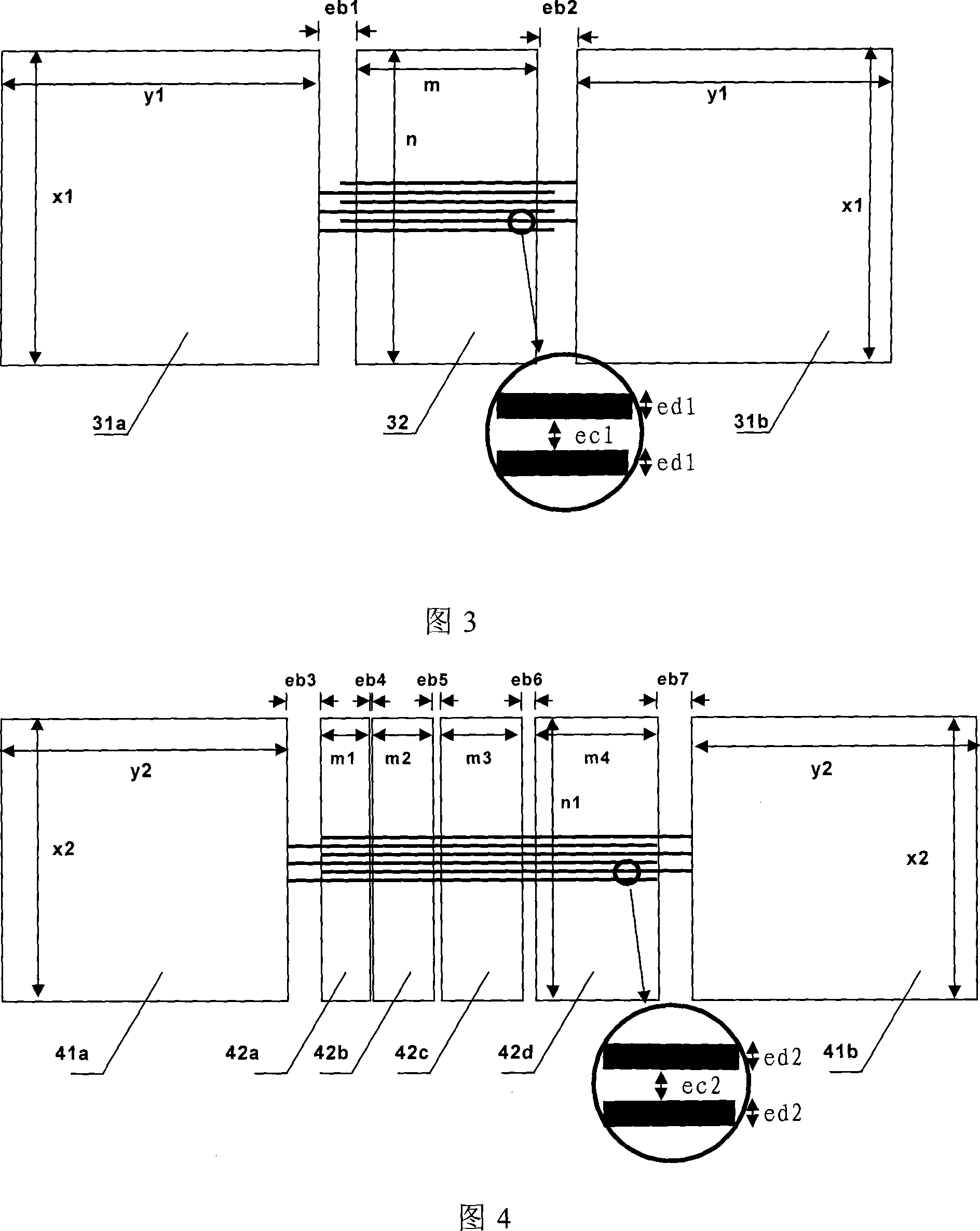
[0047] In this embodiment, the 0.13 μm copper wiring process is adopted, which is mainly used to detect the degree of influence of the erosion of the dielectric region caused by CMP on the first metal layer on the copper wiring on the fifth metal layer.
[0048] from Figure 4 It can be seen from the figure that the width x2 and length y2 of all the copper metal detection pads in the first copper metal detection pad group 41a and the second copper metal detection pad group 41b are 70 μm. On each metal layer in the chip, the copper metal detection pads of the same size, overlapping and electrically connected to each other are arranged.
[0049] This test structure comprises four copper metal block stacking units 42a, 42b, 42c and 42d, and each copper metal block stacking unit includes four consecutive, mutually overlapping For the copper metal block, the length n1 of the metal block in the four copper metal block stacking units is 70 μm, and the widths m1, m2, m3, and m4 are 1...
PUM
| Property | Measurement | Unit |
|---|---|---|
| width | aaaaa | aaaaa |
| width | aaaaa | aaaaa |
| length | aaaaa | aaaaa |
Abstract
Description
Claims
Application Information
 - R&D Engineer
- R&D Manager
- IP Professional
- Industry Leading Data Capabilities
- Powerful AI technology
- Patent DNA Extraction
Browse by: Latest US Patents, China's latest patents, Technical Efficacy Thesaurus, Application Domain, Technology Topic, Popular Technical Reports.
© 2024 PatSnap. All rights reserved.Legal|Privacy policy|Modern Slavery Act Transparency Statement|Sitemap|About US| Contact US: help@patsnap.com