Preparation for organic electroluminescence display

An organic light-emitting layer and electroluminescence technology, which is applied in the fields of electric solid-state devices, semiconductor/solid-state device manufacturing, circuits, etc., can solve problems such as difficulties, difficulty in improving yield rate, application limitations, etc. rate increase effect

Inactive Publication Date: 2011-02-16
西安文景光电科技有限公司
View PDF0 Cites 0 Cited by
  • Summary
  • Abstract
  • Description
  • Claims
  • Application Information

AI Technical Summary

Problems solved by technology

Inkjet printing methods are limited by the choice of materials and encounter problems in forming the printed structures on the substrate
Spin-coating is another commonly used method for forming polymer layers in OLED manufacturing, but when spin-coating multi-layer organics, there will be a problem that the solvent of the subsequent spin coating will damage the surface of the previous organic layer
Therefore, the application of the spin-coating method on organic electroluminescent displays is also limited.
In the evaporation process of small molecules, due to the repeated use of metal masks, it is difficult to improve the yield of patterned light-emitting layers and pixels at the same time
Evaporation methods also have difficulties in manufacturing large-scale displays

Method used


Image

  • Preparation for organic electroluminescence display
  • Preparation for organic electroluminescence display
  • Preparation for organic electroluminescence display

Examples


Embodiment 1

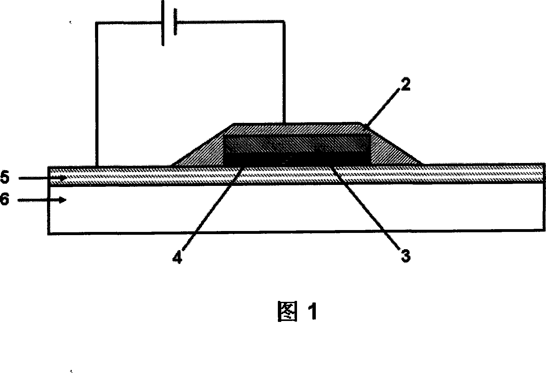
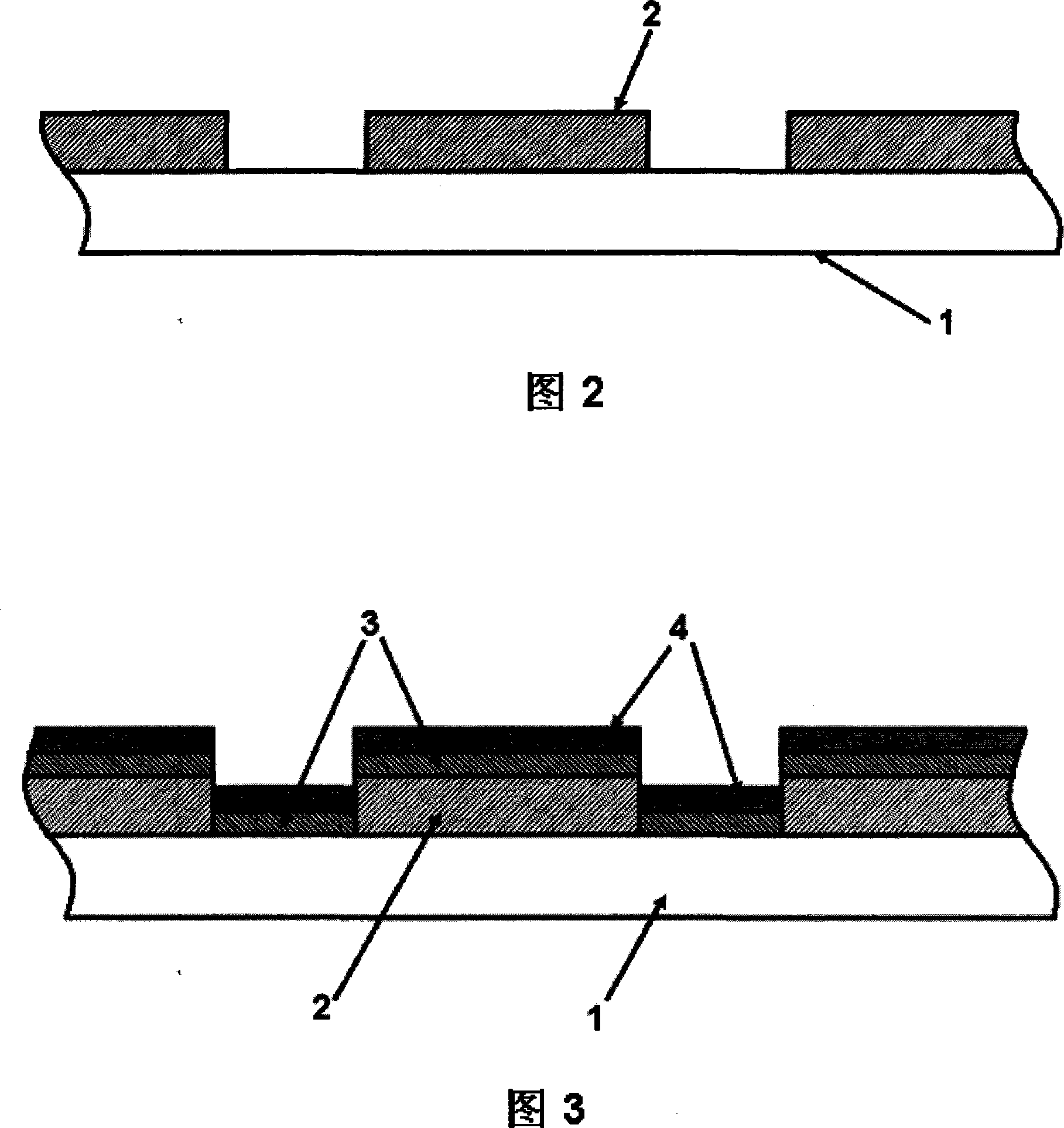
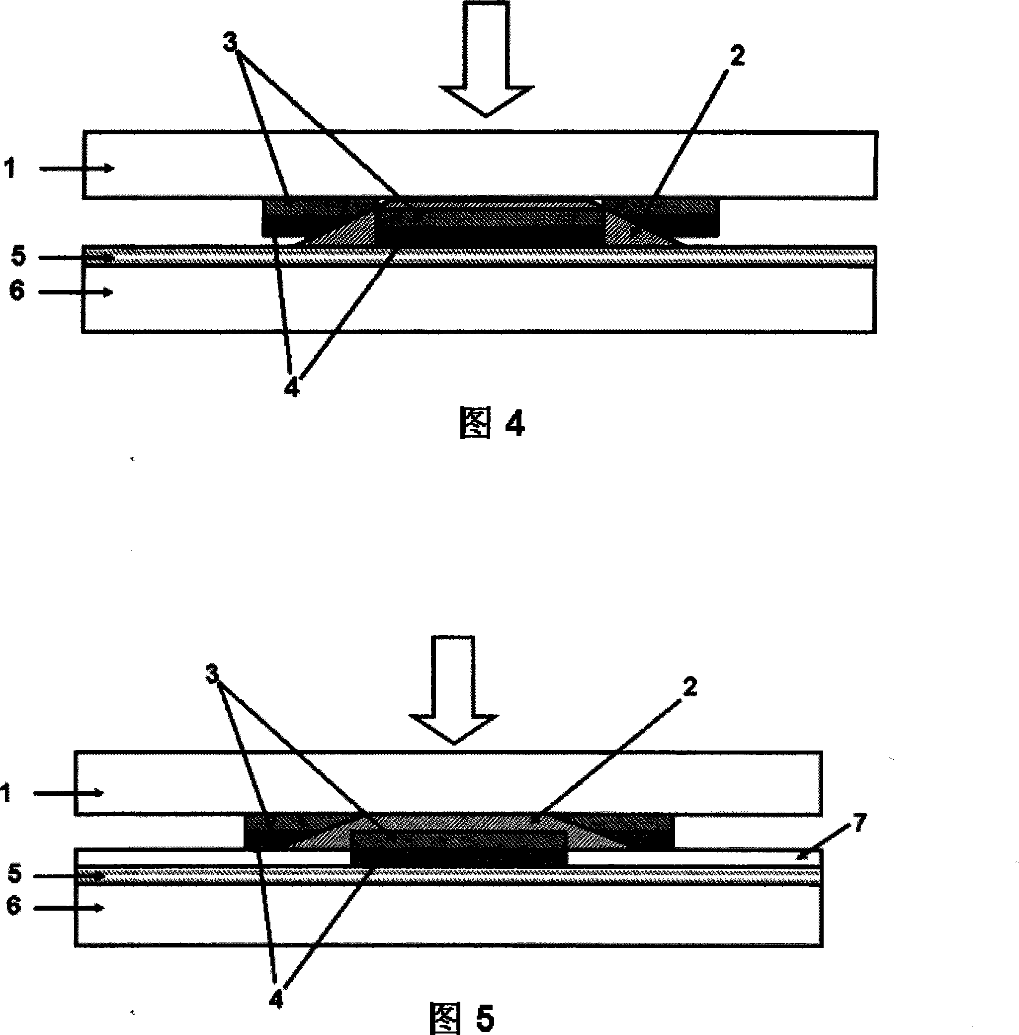
[0025] see Figure 1~4 A patterned conductive adhesive layer 2 is formed under the substrate 1 made of plastic, glass, metal or ceramic hard material or flexible material of plastic film by spin coating, screen printing or inkjet printing. The anisotropic conductive adhesive is made by mixing metal powder with a power function greater than 4eV and a polymer adhesive, and the metal powder is gold, silver, copper, aluminum, tin, indium, nickel or alloy powder thereof. On the anisotropic conductive adhesive layer 2, the first electrode layer 3 is sequentially formed by vapor deposition or sputtering, and the organic light-emitting layer 4 is formed by vapor deposition; It is formed of one or more layers of materials of metal, metal alloy or conductive oxide; the organic light-emitting layer is formed of carrier injection material, carrier transport material and light-emitting material itself. After the anisotropic conductive adhesive layer 2 of the substrate 1 is pressed against...

Embodiment 2

[0027] see figure 1 , 2 , 3, 5, using spin coating, screen printing or inkjet printing to form a patterned anisotropic conductive adhesive under the substrate 1 of hard materials such as plastics, glass, metal or ceramics or flexible materials such as plastic films. Mixture layer 2. The isotropic conductive adhesive 2 is made by mixing metal powder with a power function greater than 4eV and a polymer binder, and the metal powder is gold, silver, copper, aluminum, tin, indium, nickel or alloy powder thereof. On the isotropic conductive adhesive layer, the first electrode layer 3 is sequentially formed by evaporation or sputtering, and the organic light-emitting layer 4 is formed by evaporation; the first electrode layer is made of a metal that is conducive to carrier injection. , metal alloy or one or more layers of conductive oxide materials; the organic light-emitting layer is formed by carrier injection materials, carrier transport materials and the light-emitting material...


PUM


Abstract

The invention relates to a preparation method for an organic light-emitting display. The method is characterized in that the preparation method comprises the following concrete steps: firstly, a patterned conductive adhesive layer is formed on the lower surface of a base plate in a manner of spin coating, screen printing or ink jet printing; secondly, a first electrode layer and an organic light-emitting layer are formed on the conductive adhesive layer in sequence in a manner of evaporation or sputtering; and thirdly, one surface of the conductive adhesive layer of the base plate is pressed and fixed on the surface of a second electrode layer and is separated from the conductive adhesive layer, so as to ensure that the first electrode layer, the organic light-emitting layer and the second electrode layer form the organic light-emitting display. The method not only ensures that the yields of the patterned light-emitting layer and picture elements which are simultaneously formed are improved, but also has significant advantages in the aspect of full-color and large-size display manufacture. The method has the advantages that not only the manufacture process is simple and reliable, and the operation is convenient, but also the method is effective and economical.

Description

technical field [0001] The invention relates to a method for preparing a photoelectric device, in particular to a method for preparing an organic electroluminescence display. technical background [0002] Organic electroluminescent displays based on organic electroluminescent diode (OLED) technology have almost all the characteristics that the next-generation flat panel display technology needs to meet: very thin, able to work at a low voltage of several volts to more than ten volts, almost There is no viewing angle problem, and displays can be formed on flexible substrates, etc., so their application prospects on flat panel displays (FPDs) have attracted extensive attention from academic and industrial circles. [0003] The existing organic electroluminescent display preparation methods can be divided into two categories, one is the polymer-based wet process type, that is, organic light-emitting is formed on the substrate with pixel electrodes by using inkjet printing or sp...

Claims


Application Information

Patent Timeline
Patent Type & Authority Patents(China)
IPC IPC(8): H01L21/82H01L51/56
Inventor 黄会文苏璇宋书清
Owner 西安文景光电科技有限公司
Why Eureka
Try Eureka