
Method for detecting mask printing plate

A mask and mask technology, applied in the field of mask detection, can solve problems such as long time period

Active Publication Date: 2011-05-04
SHANGHAI HUAHONG GRACE SEMICON MFG CORP
View PDF6 Cites 0 Cited by
  • Summary
  • Abstract
  • Description
  • Claims
  • Application Information

AI Technical Summary

Problems solved by technology

[0004] The existing method can only confirm whether there are large graphic defects on the mask plate, and not only has the disadvantage of long time period, but generally needs a period of 1-2 months

Method used


Image

  • Method for detecting mask printing plate
  • Method for detecting mask printing plate
  • Method for detecting mask printing plate

Examples


Embodiment Construction

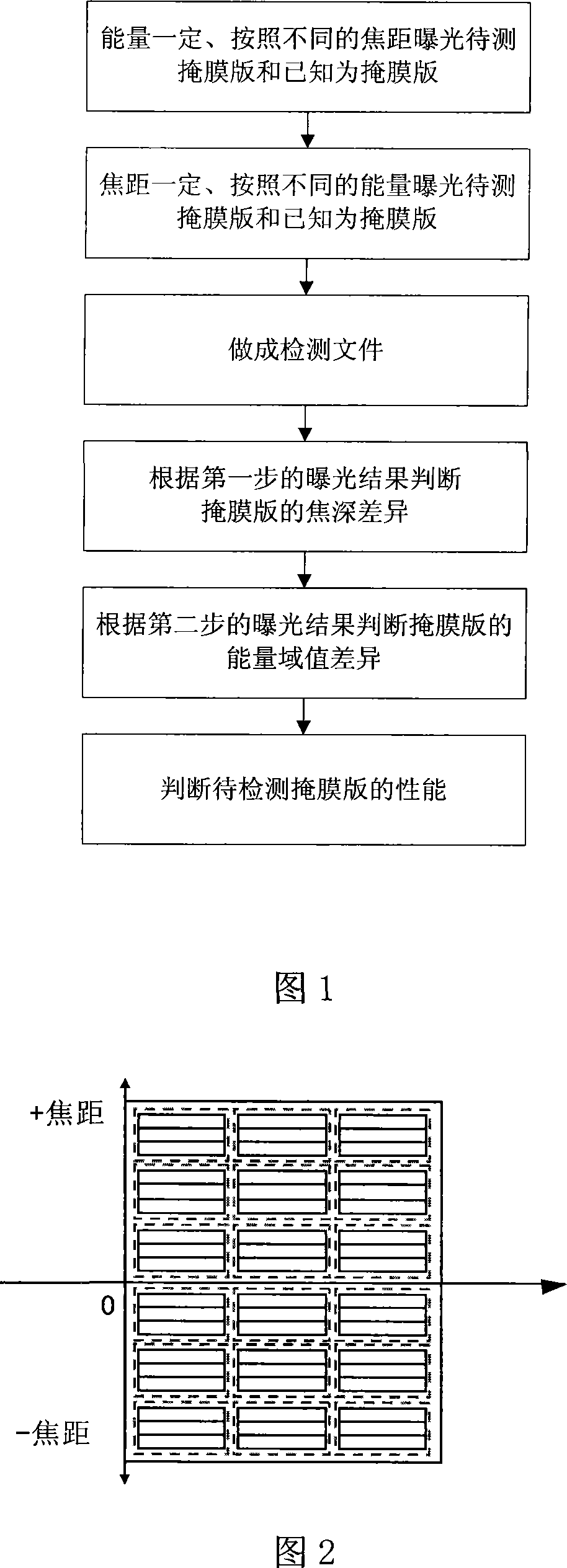
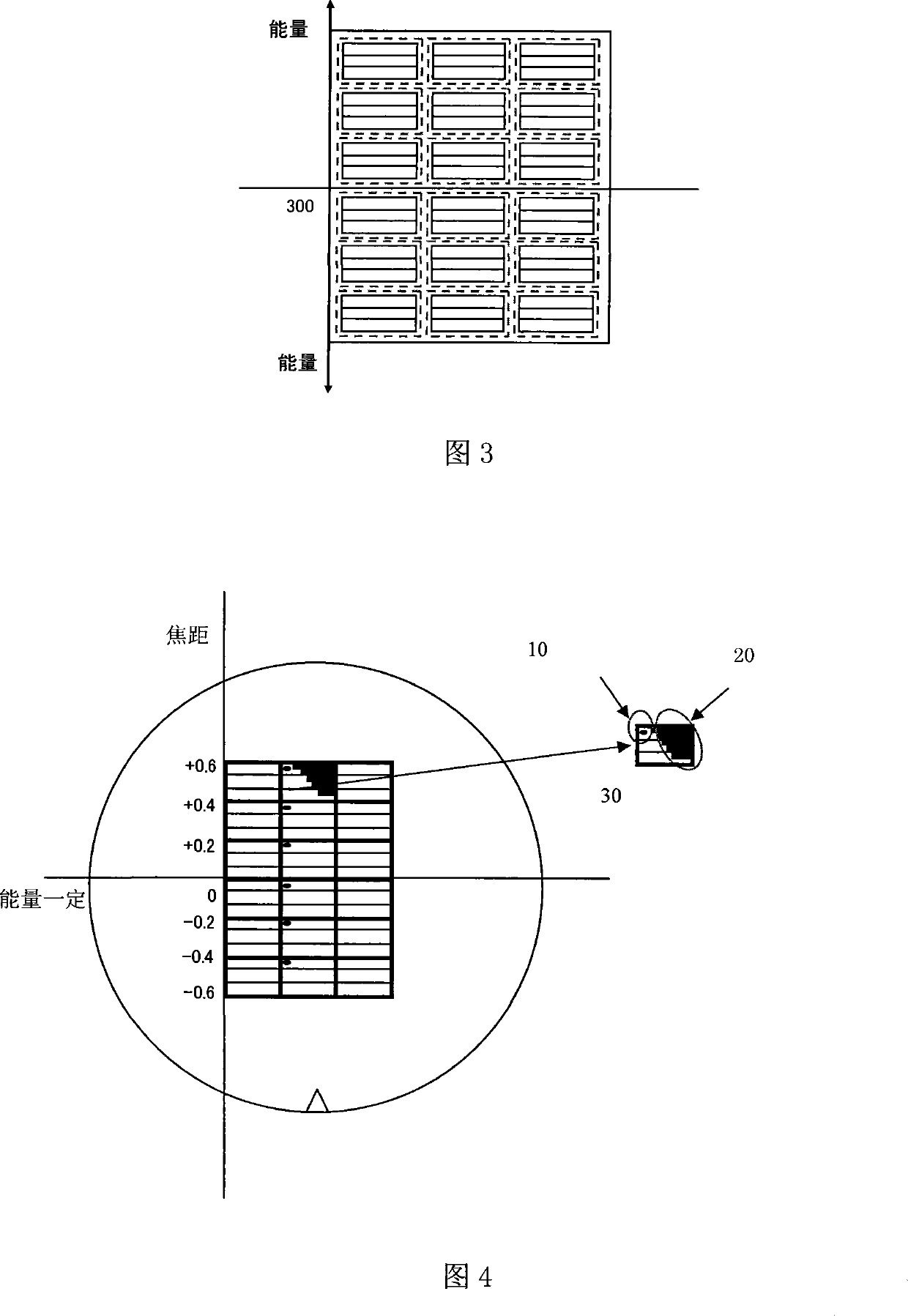
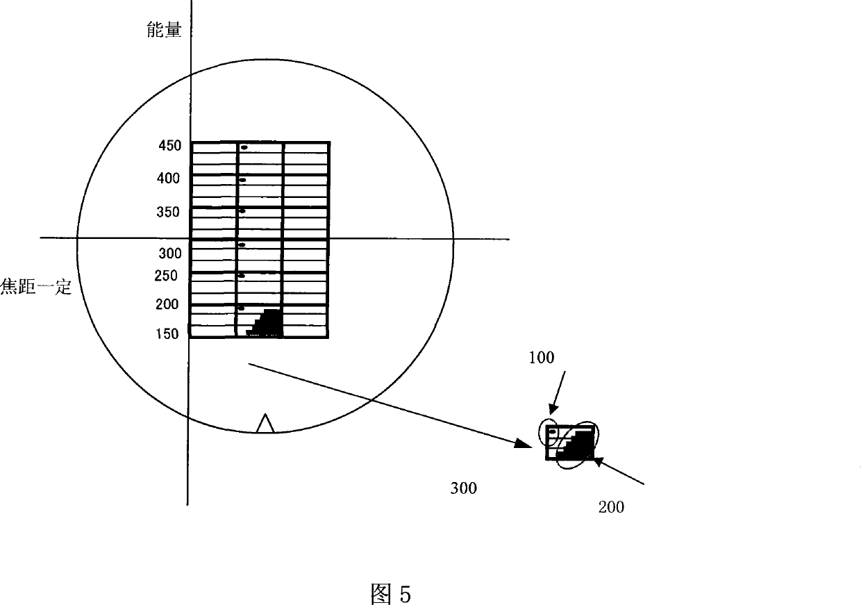
[0014] As shown in Fig. 1, the steps that the present invention detects the reticle include are: 1, the energy is certain, according to different focal lengths, simultaneously expose the reticle to be detected and the pattern known as the good reticle on the light sheet; 2, With a fixed focal length, according to different energies, the pattern of the mask to be tested and the known good mask is simultaneously exposed on the light sheet; 3. According to the exposure result of the first step, the mask to be tested and the mask known to be good The focal depth difference of the stencil, as well as the pattern and particle status of the mask; 4. Judging the energy threshold difference between the mask to be detected and the mask known to be a good product according to the exposure results of the second step, and The pattern and particle status of the mask; 5. Combine the results of the third step and the fourth step to judge the performance of the mask to be tested.

[0015] As s...


PUM


Abstract

The invention discloses a method for detecting a masking plate. The method comprises the following steps: 1, under the condition of unchanged energy, carrying out simultaneous exposure of patterns of a masking plate to be detected and a masking plate known as a non-defective product on an optical piece according to different focal lengths; 2, under the condition of unchanged focal length, carrying out the simultaneous exposure of the patterns of the masking plate to be detected and the masking plate known as the non-defective product on the optical piece according to different energy; 3, making a detection file; 4, according to exposure results of the step 1, judging focal depth difference between the masking plate to be detected and the masking plate known as the non-defective product and the patterns and condition of particles of the two masking plates; 5, according to exposure results of the step 2, judging energy domain value difference between the masking plate to be detected andthe masking plate known as the non-defective product and the patterns and the condition of the particles of the two masking plates; and 6, according to results of the step 4 and step 5, judging the performance of the masking plate to be detected. The method can reduce the workload and improve the working efficiency.

Description

technical field [0001] The invention relates to a testing method for semiconductor technology, in particular to a method for detecting a mask. Background technique [0002] Reticle The photomask used in semiconductor technology to provide circuit patterns for pattern transfer is widely used in the semiconductor field. Whether the pattern of the mask is correct or not is very important in the field of semiconductor devices, and it is also very important to detect the pattern and performance of the mask. [0003] The traditional mask pattern and particle detection is to use the special laser detection instrument for the mask to detect, and the performance evaluation of the focal depth and energy threshold of the mask is to use the mask to directly manufacture the product, and then through The product yield rate confirms whether the mask plate is normal to judge. [0004] This existing method can only confirm whether there are large graphic defects on the mask, and not only h...

Claims


Application Information

Patent Timeline
Patent Type & Authority Patents(China)
IPC IPC(8): G03F1/00G03F7/20H01L21/027H01L21/66G03F1/84
Inventor 王柳
Owner SHANGHAI HUAHONG GRACE SEMICON MFG CORP
Learn More