Micro-nano structure preparation method on metallic material surface using femtosecond laser
A metal material, femtosecond laser technology, applied in the direction of laser welding equipment, metal processing equipment, welding equipment, etc., can solve the problems of no relevant reports, material types and processing pattern limitations, etc., and achieve the effect of obvious spectral selectivity
- Summary
- Abstract
- Description
- Claims
- Application Information
AI Technical Summary
Problems solved by technology
Method used
Image
Examples
Embodiment 1
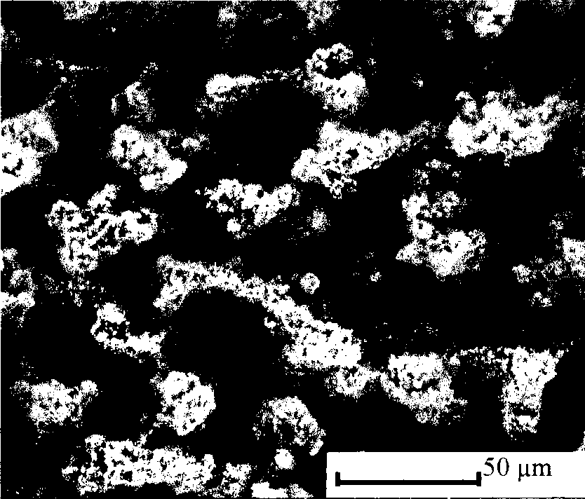
[0035] 1) Divide 10×10×2mm 3 The titanium-nickel alloy material is polished step by step with 400-800 water sandpaper, cleaned ultrasonically with deionized water, and then fixed on a three-dimensional precision mobile platform in an air environment, and the above-mentioned movement of material in spatial position;
[0036] 2) The femtosecond laser beam is used as the main optical path, and the helium-neon laser beam is used as the auxiliary optical path. After the focusing mirror reaches the surface of the metal material vertically, the femtosecond laser parameters are: pulse repetition frequency 1 kHz, pulse width 50 femtoseconds, pulse center wavelength 800 nanometers, beam polarization direction is linear polarization;
[0037] 3) Turn off the femtosecond laser beam so that only the helium-neon laser beam is irradiated at a certain position on the surface of the above-mentioned material, and then place a beam splitter at an angle of 45 degrees on the optical path away fro...
Embodiment 2
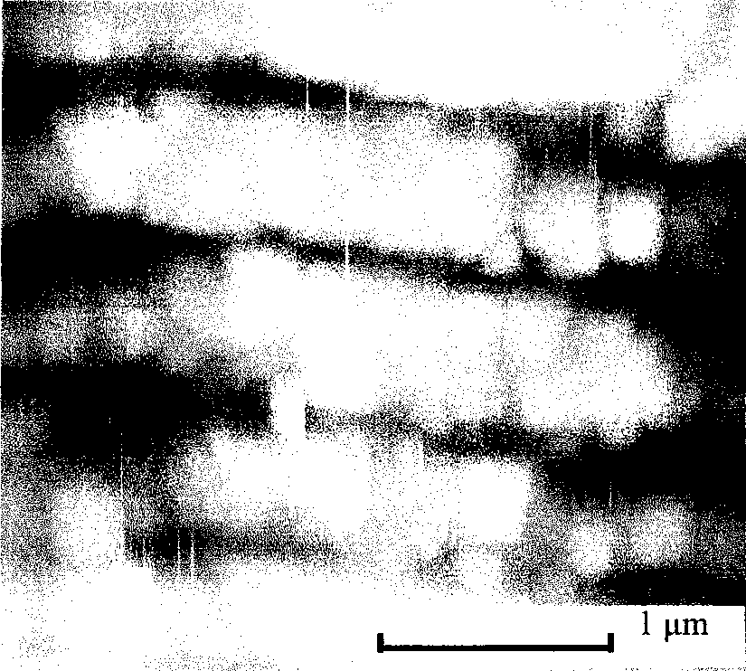
[0048] Except that the single pulse energy of the incident femtosecond laser is adjusted to 50 microjoules, other technical steps and process conditions are the same as those in Example 1. In this case, it was observed that the surface self-organization of the titanium alloy material after femtosecond laser irradiation produced a periodic stripe-like microstructure, and its atomic force micrograph is shown in figure 2 shown. The direction of the stripes of this microstructure is perpendicular to the polarization direction of the incident laser light and the scanning direction of the sample, the average interval of the stripes is 630 nanometers, the height of the stripes is about 150 nanometers, and the width is about 290 nanometers. More importantly, a large number of irregularly shaped solid particles are covered on this subwavelength grating-like microstripes, and their geometric size distribution is between tens and two hundred nanometers, which can be obtained in titanium...
Embodiment 3
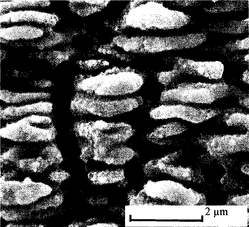
[0052] Except that the energy of the incident femtosecond laser pulse is adjusted to 150 microjoules, other technical steps and process conditions are the same as in Example 1. In this case, it was observed that the surface self-organization of the titanium-nickel alloy material after femtosecond laser irradiation produced a honeycomb-like composite structure composed of subwavelength gratings and nanopores, and its scanning electron micrograph is shown in image 3 shown. Similar to the case in Example 2, the stripe direction in this composite structure is perpendicular to the laser polarization direction and the sample scanning direction, but the stripe interval varies between 400–600 nm, and the length of each group of stripes is shortened to about 1 μm . In addition, compared with the case of the microcavity in Example 1, the size of the cavities in this composite structure is significantly smaller, with a diameter of about 500 nanometers, and their distribution density in...
PUM
| Property | Measurement | Unit |
|---|---|---|
| width | aaaaa | aaaaa |
Abstract
Description
Claims
Application Information
 - R&D
- Intellectual Property
- Life Sciences
- Materials
- Tech Scout
- Unparalleled Data Quality
- Higher Quality Content
- 60% Fewer Hallucinations
Browse by: Latest US Patents, China's latest patents, Technical Efficacy Thesaurus, Application Domain, Technology Topic, Popular Technical Reports.
© 2025 PatSnap. All rights reserved.Legal|Privacy policy|Modern Slavery Act Transparency Statement|Sitemap|About US| Contact US: help@patsnap.com


