Printed circuit board

A technology of printed circuit substrates and substrates, applied in the direction of printed circuits, printed circuits, printed circuit manufacturing, etc., can solve the problems of long process and large environmental load, and achieve the effects of reducing intermediate inventory, being environmentally friendly, and shortening the production process

Inactive Publication Date: 2008-12-10
SMK CO LTD
View PDF1 Cites 1 Cited by
  • Summary
  • Abstract
  • Description
  • Claims
  • Application Information

AI Technical Summary

Problems solved by technology

[0004] Therefore, a process of printing an etching resist layer by screen printing, a process of curing a protective film by UV, etc., and an etching and peeling process of copper foil are required, resulting in not only a long process, but also a large environmental load due to the use of chemicals. Issues such as drainage treatment

Method used


Image

  • Printed circuit board
  • Printed circuit board

Examples


Embodiment Construction

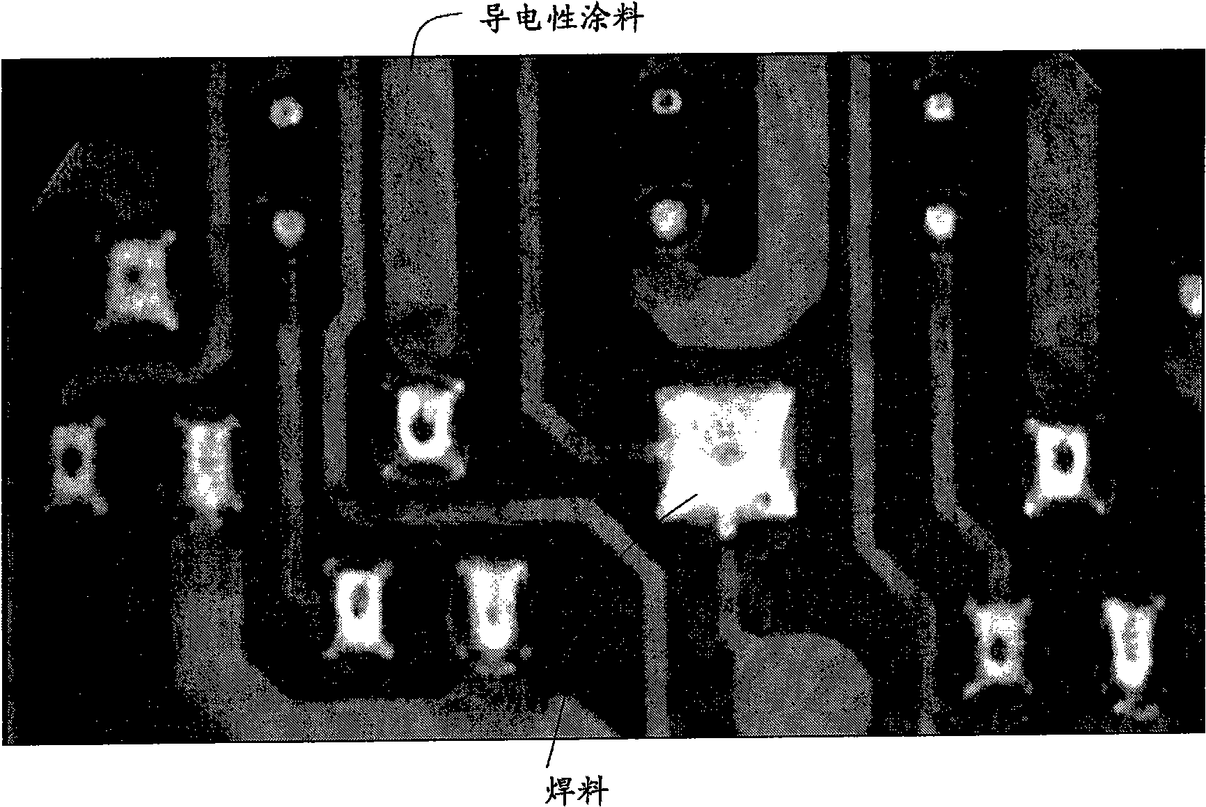
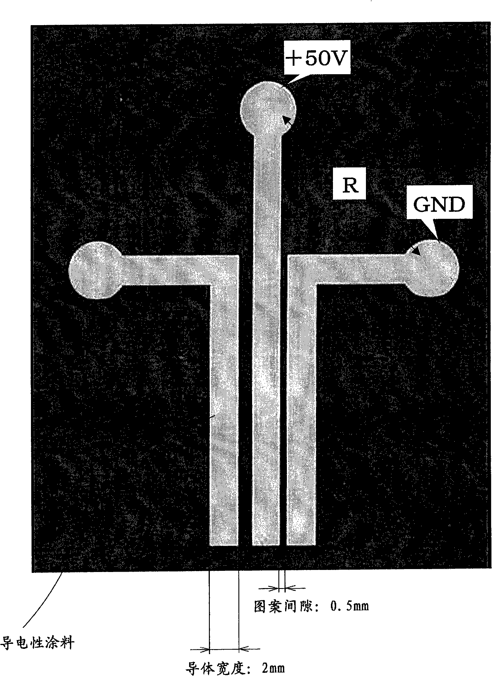
[0024] The printed circuit board according to the present invention is applicable to various electronic boards, but in this example, the case where it is used as a remote control board for remote operation of electric and electronic equipment is evaluated as an example, and will be described below.

[0025] As a phenolic paper substrate material for impregnating a paper substrate with a phenolic resin, the following two types were prepared: substrate material A (manufactured by Richang Industry Co., Ltd., PS-1131) with a thickness of 1.6 mm and an absorption rate of 2.0%; 0.8% of substrate material B (manufactured by Risho Kogyo Co., Ltd., PS-1143S).

[0026] As substrate materials for resin-impregnated paper substrates, in addition to phenolic paper substrate materials, epoxy paper substrate materials impregnated with epoxy resin are also readily available, but phenolic paper substrate materials are usually cheaper.

[0027] In a word, in the present invention, there is no ne...


PUM

PropertyMeasurementUnit
water absorptionaaaaaaaaaa

Abstract

This invention is related to a printed circuit board. The target of this invention is to provide a cheap printed circuit board with reduced manufacturing process, wherein a circuit is printed on a circuit board material, which does not have a copper foil layer and does have a paper base material after impregnating with a resin and using an electroconductive coating material. The board material preferably is a paper phenol board material, wherein the paper base material is impregnated with phenol resin, on which a resist layer is formed and a circuit is printed on the resist layer using an electroconductive coating material.

Description

technical field [0001] The present invention relates to a printed circuit substrate printed with conductive paint to form a circuit. Background technique [0002] As printed circuit boards that have been widely used in the past, copper-clad boards in which copper foil is laminated on a phenolic board material or a glass epoxy board material are used. [0003] When forming a wiring pattern on this substrate material, an etching resist layer is formed on the part where the copper foil layer is to be left, and the copper foil on other parts is removed by chemical etching. [0004] Therefore, a process of printing an etching resist layer by screen printing, a process of curing a protective film by UV, etc., and an etching and peeling process of copper foil are required, resulting in not only a long process, but also a large environmental load due to the use of chemicals. Issues such as drainage treatment. [0005] Therefore, the applicant of the present application has intensi...

Claims


Application Information

Patent Timeline
Patent Type & Authority Applications(China)
IPC IPC(8): H05K1/00H05K1/03H05K3/12
CPCH05K1/0366H05K1/095H05K3/386H05K2201/0284H05K1/03
Inventor 笠置延生
Owner SMK CO LTD
Why Eureka
Try Eureka