
Method for accomplishing sub-wavelength interference photolithography utilizing multiple layer metal dielectric-coating structure

A multi-layer metal, interference lithography technology, applied to the originals for optomechanical processing, photosensitive materials for optomechanical equipment, microlithography exposure equipment, etc., can solve the problem of uneven fringe visibility, short interference area, Problems such as limited transmission distance

Inactive Publication Date: 2008-09-10
INST OF OPTICS & ELECTRONICS - CHINESE ACAD OF SCI
View PDF0 Cites 12 Cited by
  • Summary
  • Abstract
  • Description
  • Claims
  • Application Information

AI Technical Summary

Problems solved by technology

[0002] The realization of sub-wavelength interference lithography by using the short-wavelength characteristics of surface plasmon (SP) has been published in Surface Plasmon Interference Nanolithography, NANO LETTERS, 2005, Vol, 5, No.5, 957-961; Large-area surface-plasmon polariton interference lithography, 2006 / Vol.31, No.17 / OPTICS LETTERS 2613-2615 and many other documents mentioned; however, two key issues have not been resolved: surface plasmon wave excitation and the area and uniformity of interference lines Because the surface plasmon wave interference wavelength is much smaller than the vacuum wavelength, and the existing optical materials have a limited refractive index, the excitation of the surface plasmon wave by the prism method cannot obtain a very short surface plasmon wave wavelength, so the interference pattern period is relatively large ; In the literature NANO LETTERS, 2005, Vol.5, No.5, 957-961, the surface plasmon waves that are transmitted in opposite directions are excited by introducing finite-length gratings or sub-wavelength slit structures on both sides of the interference region, which can avoid the excitation light The influence of the zero-order direct component on the interference field, but the problem is that due to the limited propagation distance of the excited surface plasmon wave in the interference area, the interference area is very short, and the visibility of the fringes is uneven, which greatly limits its practicability

Method used


Image

  • Method for accomplishing sub-wavelength interference photolithography utilizing multiple layer metal dielectric-coating structure
  • Method for accomplishing sub-wavelength interference photolithography utilizing multiple layer metal dielectric-coating structure
  • Method for accomplishing sub-wavelength interference photolithography utilizing multiple layer metal dielectric-coating structure

Examples


Embodiment Construction

[0037] The present invention will be described in detail below in conjunction with the accompanying drawings and specific embodiments.

[0038] The present invention utilizes a multilayer metal dielectric film structure to realize a method for subwavelength interference lithography, and its specific implementation steps are as follows:

[0039] (1) Choose quartz as the base material, such as figure 1 shown;

[0040] (2) Spin-coat a layer of resist AZ3100 on the surface of the substrate with a thickness of 100nm, such as figure 2 shown;

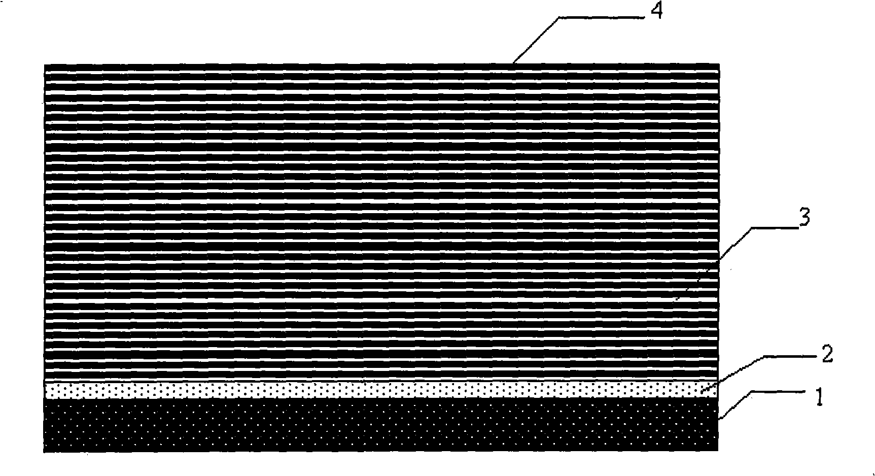
[0041] (3) Metal silver film and magnesium fluoride film are vapor-deposited alternately on the resist surface, the thickness of silver layer is 20nm, the thickness of magnesium fluoride is 30nm, wherein silver layer and magnesium fluoride layer are respectively 35 layers, obtain structure Such as image 3 shown;

[0042] (4) Design and fabricate the mask structure. It is proposed to obtain photolithography lines with a line width of 32n...


PUM

PropertyMeasurementUnit
thicknessaaaaaaaaaa
thicknessaaaaaaaaaa
widthaaaaaaaaaa

Abstract

A method for utilizing multilayer metal dielectric film structure to realize the sub-wavelength interference lithography is characterized by the following steps of selecting a substrate material; coating an anticorrosion agent on the surface of the substrate; carrying out the alternate vapor deposition of a metal material film and a dielectric material film on the surface of the anticorrosion agent to form a metal layer and a dielectric layer which are arranged alternately; designing and arranging a periodic structure pattern mask on the surface of the structure which is obtained by the above step; carrying out the exposure of the obtained structure; removing the mask structure after the finish of the exposure; further removing the material of the metal layer and the material of the dielectric layer; arranging the obtained structure in a developing liquid which is matched with the anticorrosion agent for carrying out the development; carrying out the dry etching of the structure after the development and transferring the structure on the substrate; removing the residual anticorrosion agent on the surface of the structure and obtaining a final sub-wavelength periodic structure pattern; the utilization of the method of the invention can realize the periodic structure pattern with a large area, evenness and the period of which is below the wavelength.

Description

technical field [0001] The invention provides a method for performing sub-wavelength interference lithography, in particular to a method for realizing sub-wavelength interference lithography by using a multi-layer metal dielectric film structure. Background technique [0002] The realization of sub-wavelength interference lithography by using the short-wavelength characteristics of surface plasmon (SP) has been published in Surface Plasmon Interference Nanolithography, NANO LETTERS, 2005, Vol, 5, No.5, 957-961; Large-area surface-plasmon polariton interference lithography, 2006 / Vol.31, No.17 / OPTICS LETTERS 2613-2615 and many other documents mentioned; however, two key issues have not been resolved: surface plasmon wave excitation and the area and uniformity of interference lines Because the surface plasmon wave interference wavelength is much smaller than the vacuum wavelength, and the existing optical materials have a limited refractive index, the excitation of the surface ...

Claims


Application Information

Patent Timeline
Patent Type & Authority Applications(China)
IPC IPC(8): G03F7/20G03F7/26G03F7/004G03F1/08G03F1/00G03F1/80
Inventor 王长涛徐挺史立芳赵延辉崔建华杜春雷罗先刚
Owner INST OF OPTICS & ELECTRONICS - CHINESE ACAD OF SCI
Learn More