Negative fluorine-contained photoresist composition and its application in polymer optical waveguide device
A technology of photoresist and composition, applied in the direction of optical waveguide light guide, light guide, optical element, etc., can solve the problem of large light loss and so on
- Summary
- Abstract
- Description
- Claims
- Application Information
AI Technical Summary
Problems solved by technology
Method used
Image


Examples
Embodiment 1
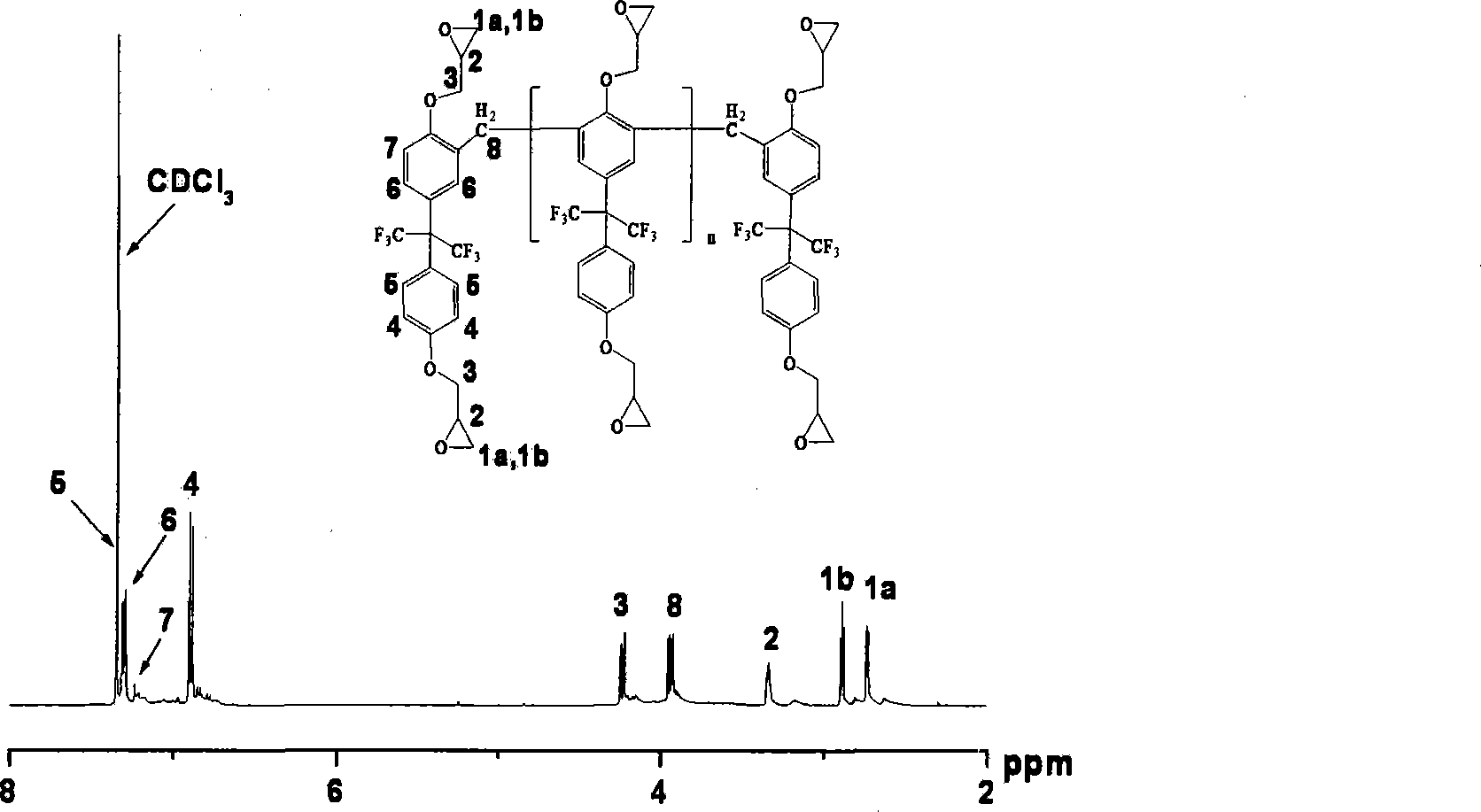
[0033] Dissolve 10 g of fluorinated bisphenol A in excess formaldehyde (5.4 g, 40% formaldehyde solution), under the catalysis of concentrated sulfuric acid (0.39 g), raise the temperature to 75 ° C, and react at this temperature for 6 h. Rinse with a large amount of distilled water until the solution becomes neutral (pH value is 7), and put it into a vacuum drying oven for dehydration. The epichlorohydrin (50g) that then adds in the product, heats up and melts and catalyzes with solid caustic soda, adds 0.25g NaOH every 0.5h, and reacts altogether for 8 hours. After the addition, keep at 60°C for 6h to complete the cyclization reaction. Steam the unreacted epichlorohydrin, then extract with toluene, filter and remove benzene to obtain fluorine-containing epoxy resin that can be used to prepare polymer optical waveguide devices, such as image 3 The structural formula of this example product. The yield is 91.3%, Mn=1071, Mw / Mn=1.8281, 1 H NMR (500MHz, CDCl 3 , TMS): 66.88-...
Embodiment 2
[0036] 5.000g of fluorine-containing epoxy resin (obtained by the method in Example 1, Mn=1071, Mw / Mn=1.8281), 0.500g of triphenylhexafluorosulfonium phosphate and 3.667g of cyclopentanone were mixed to obtain a A photoresist solution.
[0037] On a silicon wafer coated with a silicon dioxide film (with H 2 SO 4 :H 2 o 2 =7:3 solution has been processed) spin-coat this photoresist solution on, the rotating speed is 500rpm, 9s, 1000rpm, 30s; Bake 20min at 95 ℃; Photoresist film thickness is about 8 μm, mask (strip shape Waveguide mask, 3×5cm 2 ) and UV exposure (power 1000w, wavelength 200-400nm) for 60s; middle baking at 120°C for 60min; development in propylene glycol monomethyl ether acetate (PGMEA) for 20s; post-baking at 130°C for 30min to obtain Straight waveguide devices.
Embodiment 3
[0039] 5.000g of fluorine-containing epoxy resin (obtained by the method in Example 1, Mn=1071, Mw / Mn=1.8281), 0.500g of iodonium diphenylhexafluorophosphate and 3.667g of cyclopentanone were mixed to obtain a A photoresist solution.
[0040] On a silicon wafer coated with a silicon dioxide film (with H 2 SO 4 :H 2 o 2 =7:3 solution processed) spin-coat this photoresist solution, the rotating speed is 500rpm, 9s, 1000rpm, 30s, the thickness of photoresist layer is about 8 μ m; Bake 30min under 80 ℃; Mask (strip waveguide Mask plate, 3×5cm 2 ) and UV exposure (power 1000w, wavelength 200-400nm) for 60s; bake at 120°C for 60min; develop in butyrolactone for 20s; then bake at 130°C for 30min. The scanning electron micrographs of the straight waveguide are as follows: figure 2 As shown, the surface is regular and the sidewall is steep. And it is measured that at a wavelength of 1550nm, the optical loss of the 6×6μm straight waveguide strip is only 0.21dB / cm.
PUM
| Property | Measurement | Unit |
|---|---|---|
| dispersity | aaaaa | aaaaa |
| glass transition temperature | aaaaa | aaaaa |
Abstract
Description
Claims
Application Information
 - Generate Ideas
- Intellectual Property
- Life Sciences
- Materials
- Tech Scout
- Unparalleled Data Quality
- Higher Quality Content
- 60% Fewer Hallucinations
Browse by: Latest US Patents, China's latest patents, Technical Efficacy Thesaurus, Application Domain, Technology Topic, Popular Technical Reports.
© 2025 PatSnap. All rights reserved.Legal|Privacy policy|Modern Slavery Act Transparency Statement|Sitemap|About US| Contact US: help@patsnap.com