


Quick Research
Generate reliable direction feasibility study reports for your R&D in just a few steps.

Technical Q&A
Discover and master advanced knowledge NOW. Basics, ideas, possibilities, all at once.

Find Solutions
As an expert in R&D theories, this can generate solutions to your technical problems instantly.

Evaluate Feasibility
Analyze your overall solution with one click, know your potential R&D risks in advance.

Monitor Landscape
Get weekly tech updates, stay abreast of the latest tech innovations and key insights.
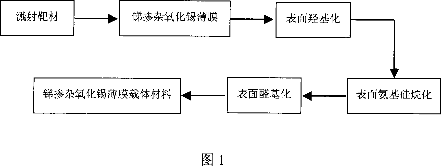
Method for preparing antimony-doping tin oxide thin film carrier material
An antimony-doped tin oxide and carrier material technology, applied in metal material coating process, ion implantation plating, coating and other directions, can solve the problem of not fully satisfying the conductivity and chemical stability of carrier materials and the stability of biological signal detection sensitivity chips It has problems such as poor performance and expensive biological signal detection equipment, and achieves the effects of strong specific label-free electrical detection, high-sensitivity label-free electrical detection, and low resistivity.
- Summary
- Abstract
- Description
- Claims
- Application Information
AI Technical Summary
Problems solved by technology
Method used
Image

Examples
Embodiment 1
[0024] (1) Antimony oxide (Sb) with a purity of 99.99% 2 O 3 ) and tin oxide (SnO 2 ) powder is pressed into a billet, and then sintered at 1300°C to form an antimony-doped tin oxide sputtering target. The Sb in the target 2 O 3 The mass percentage (wt.%) is 4%, SnO 2 The mass percentage (wt.%) is 96%; the size of the target is 60mm in diameter and 6mm in thickness. Before sputtering, the surface of the target is polished with sandpaper, then cleaned with analytical pure acetone and deionized water, and then placed in In an oven, keep warm at 120°C for 3 hours to remove surface oil and other impurities;
[0025] (2) Use ordinary glass slides as the film substrate material, fully wash them with analytical pure acetone and deionized water before sputtering, then put them in an oven, and keep them warm at 80°C for 2 hours;
[0026] (3) Install and put the target material and glass slide pretreated in steps (1) and (2) into the magnetron sputtering apparatus, first pre-sputte...
Embodiment 2
[0032] (1) antimony oxide (Sb) with a purity of 99.99% 2 O 3 ) and tin oxide (SnO 2 ) powder is pressed into a billet, and then sintered at 1300°C to form an antimony-doped tin oxide sputtering target. The Sb in the target2 O 3 The mass percentage (wt.%) is 4%, SnO 2 The mass percentage (wt.%) of the target material is 96%; the size of the target material is 60mm in diameter and 6mm in thickness. Before sputtering, the surface of the target material is sanded with sandpaper, then cleaned with analytical pure acetone and deionized water, and then placed in In an oven, keep the temperature at 120 °C for 3 hours to remove impurities such as oil stains on the surface;
[0033] (2) Use a common glass slide as the film base material, fully clean it with analytically pure acetone and deionized water before sputtering, and then put it into an oven and keep it at 80°C for 2 hours;
[0034] (3) Install and put the pre-treated target and glass slides in steps (1) and (2) into the mag...
Embodiment 3
[0040] (1) Antimony oxide (Sb) with a purity of 99.99% 2 O 3 ) and tin oxide (SnO 2 ) After the powder is pressed into a billet, it is sintered at 1400 °C to form an antimony-doped tin oxide sputtering target. 2 O 3 The mass percentage (wt.%) is 10%, SnO 2 The mass percentage (wt.%) of the target material is 90%; the size of the target material is 60mm in diameter and 6mm in thickness. Before sputtering, the surface of the target material is sanded with sandpaper, then cleaned with analytical pure acetone and deionized water, and then placed in In an oven, keep the temperature at 120 °C for 3 hours to remove impurities such as oil stains on the surface;
[0041] (2) Use a common glass slide as the film base material, fully clean it with analytically pure acetone and deionized water before sputtering, and then put it into an oven and keep it at 80°C for 2 hours;
[0042] (3) Install and put the pre-treated target and glass slides in steps (1) and (2) into the magnetron spu...
PUM
| Property | Measurement | Unit |
|---|---|---|
| electrical resistivity | aaaaa | aaaaa |
| thickness | aaaaa | aaaaa |
| surface roughness | aaaaa | aaaaa |
Abstract
Description
Claims
Application Information
 - R&D Engineer
- R&D Manager
- IP Professional
- Industry Leading Data Capabilities
- Powerful AI technology
- Patent DNA Extraction
Browse by: Latest US Patents, China's latest patents, Technical Efficacy Thesaurus, Application Domain, Technology Topic, Popular Technical Reports.
© 2024 PatSnap. All rights reserved.Legal|Privacy policy|Modern Slavery Act Transparency Statement|Sitemap|About US| Contact US: help@patsnap.com