
Method for improving defect of polysilicon

A polysilicon and defect technology, applied in the manufacturing of electrical components, electrical solid-state devices, semiconductor/solid-state devices, etc., can solve problems such as electrical failure, residual silicon nitride layer, unevenness, etc., and achieve the effect of improving electrical performance

Inactive Publication Date: 2008-06-11
SEMICON MFG INT (SHANGHAI) CORP +1
View PDF1 Cites 0 Cited by
  • Summary
  • Abstract
  • Description
  • Claims
  • Application Information

AI Technical Summary

Problems solved by technology

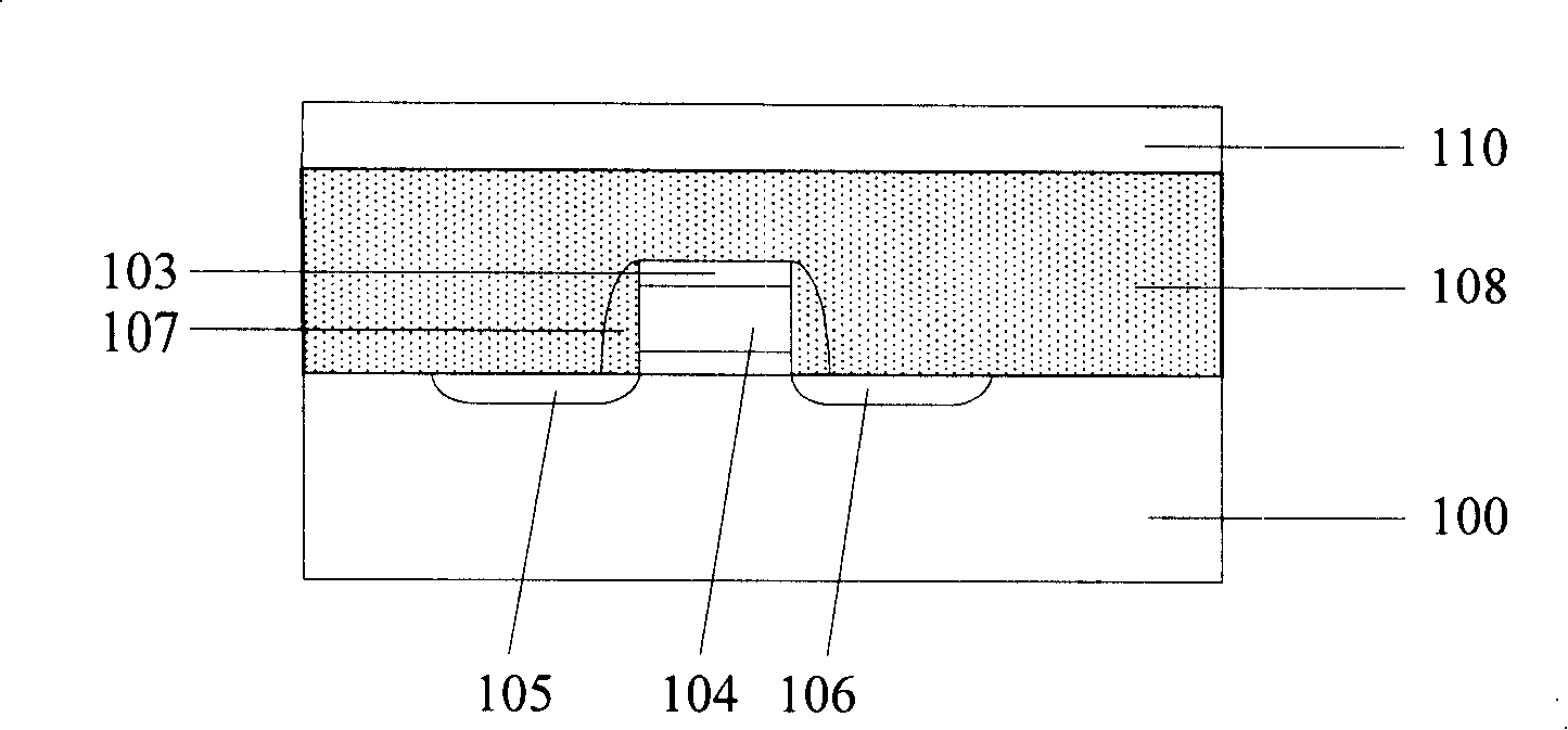
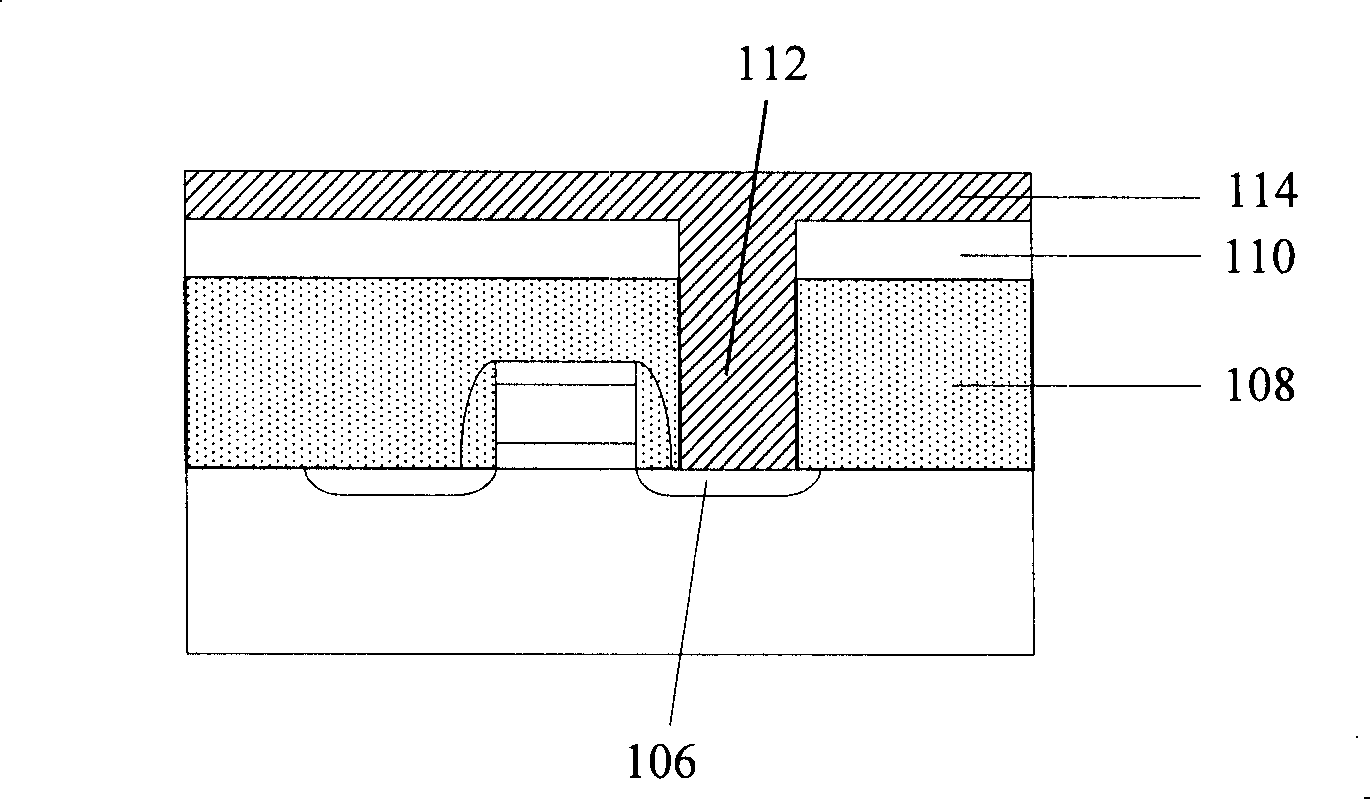
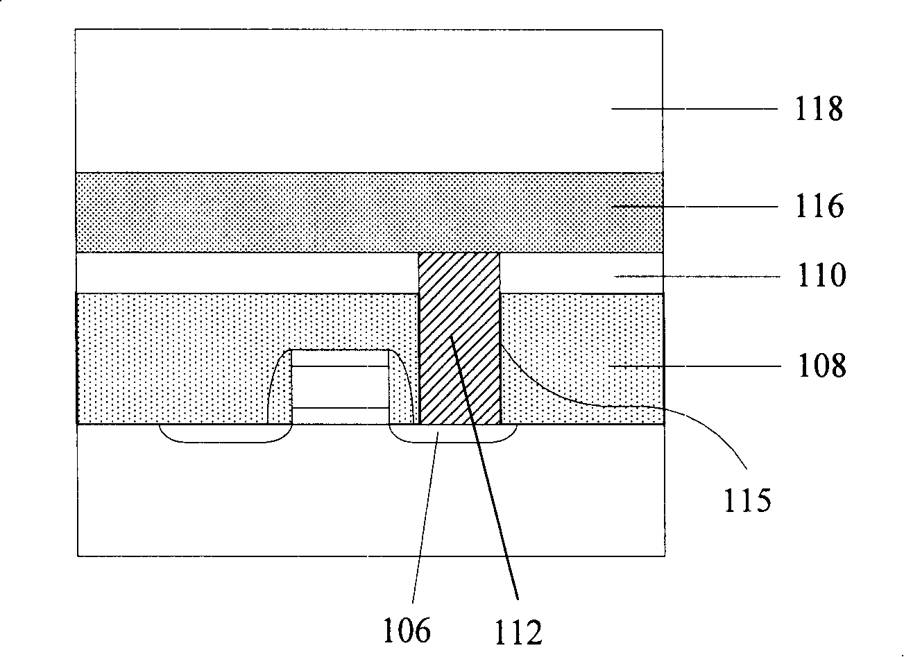
[0012] The problem solved by the present invention is to provide a method for improving polysilicon defects, to prevent the inability to etch the nitriding due to hot standard cleaning solution No. 1 (HSC1) and buffered oxide etching solution (BOE) when etching the interlayer dielectric layer. Silicon layer, resulting in the residue of the silicon nitride layer, which will cause voids or unevenness when the subsequent film is filled; at the same time, because the hot standard cleaning solution No. 1 (HSC1) will react with the polysilicon plug, resulting in defects in the polysilicon plug , leading to electrical failure

Method used


Image

  • Method for improving defect of polysilicon
  • Method for improving defect of polysilicon
  • Method for improving defect of polysilicon

Examples


Embodiment Construction

[0027]In the prior art, when the polysilicon layer is formed in the process of making DRAM capacitors, since the material of the first interlayer dielectric layer is tetraethyl orthosilicate, the material of the second interlayer dielectric layer is borophosphosilicate glass, and the dry method The etch rate of the etched gas to tetraethyl orthosilicate and borophosphosilicate glass is inconsistent, resulting in a difference in the opening width of the first interlayer dielectric layer and the second interlayer dielectric layer, so it is necessary to use hot standard cleaning solution No. 1 (HSC1 ) to etch the opening widths of the first interlayer dielectric layer and the second interlayer dielectric layer to be the same, but the hot standard cleaning solution No. 1 (HSC1) will react with the polysilicon plug, causing defects in the polysilicon plug, which in turn leads to Electrical failure. At the same time, when the hot standard cleaning solution No. 1 (HSC1) and the buffe...


PUM


Abstract

A polysilicon defect improving method comprises the following procedures that: a silicon dioxide layer is formed on a silicon substrate; a polysilicon attaching plug is formed on the silicon dioxide layer and runs through the silicon dioxide layer; a silicon nitride layer is formed on the silicon dioxide layer and is covered with the polysilicon attaching plug; an interlevel medium layer is formed on the silicon nitride layer; the interlevel medium layer on the upper part of the polysilicon attaching plug is etched to form an opening; the silicon nitride layer in the opening is etched to expose the polysilicon attaching plug; the opening is filled with polysilicon and is communicated with the polysilicon attaching plug. Through the procedures, the reaction between thermal standard cleaning liquid No 1 and the polysilicon attaching plug can not be produced because of the protection of the silicon nitride layer; as the silicon nitride layer is etched finally, therefore, the silicon nitride layer is not exposed to make the subsequent filling flat.

Description

technical field [0001] The invention relates to a manufacturing method of a semiconductor storage device, in particular to a method for improving polysilicon defects in the capacitance process of a dynamic random access memory. Background technique [0002] DRAM is a widely used integrated circuit component. Most of the DRAMs commonly used in production lines are composed of a transistor and a capacitor. Capacitors are used to store charges to provide electronic information, and they should have a large enough capacitance to avoid data loss and reduce the frequency of charging updates. [0003] With the continuous increase of integration in the integrated circuit manufacturing process, it has become a trend to increase the integration density of DRAM. However, the higher the density of DRAM storage cells, the area that capacitors can use in DRAM storage cells smaller. In order to reduce the area of ​​capacitors while still maintaining a reliable standard, it is important ...

Claims


Application Information

Patent Timeline
Patent Type & Authority Applications(China)
IPC IPC(8): H01L21/768H01L21/8242H10B12/00
CPCH01L21/31111H01L27/10852H01L21/31116H10B12/033
Inventor 杨芸杨振良金贤在王刚宁
Owner SEMICON MFG INT (SHANGHAI) CORP
Learn More