Pi type CoSb3 based thermoelectric converting device and method for producing the same
A technology of thermoelectric conversion devices and thermoelectric devices, applied in the manufacture/processing of thermoelectric devices, parts of thermoelectric devices, thermoelectric devices using only Peltier or Seebeck effect, etc., can solve problems such as welding difficulties, achieve simple welding, reduce heat Stress, the effect of achieving thermal matching
- Summary
- Abstract
- Description
- Claims
- Application Information
AI Technical Summary
Problems solved by technology
Method used
Image
Examples
Embodiment 1
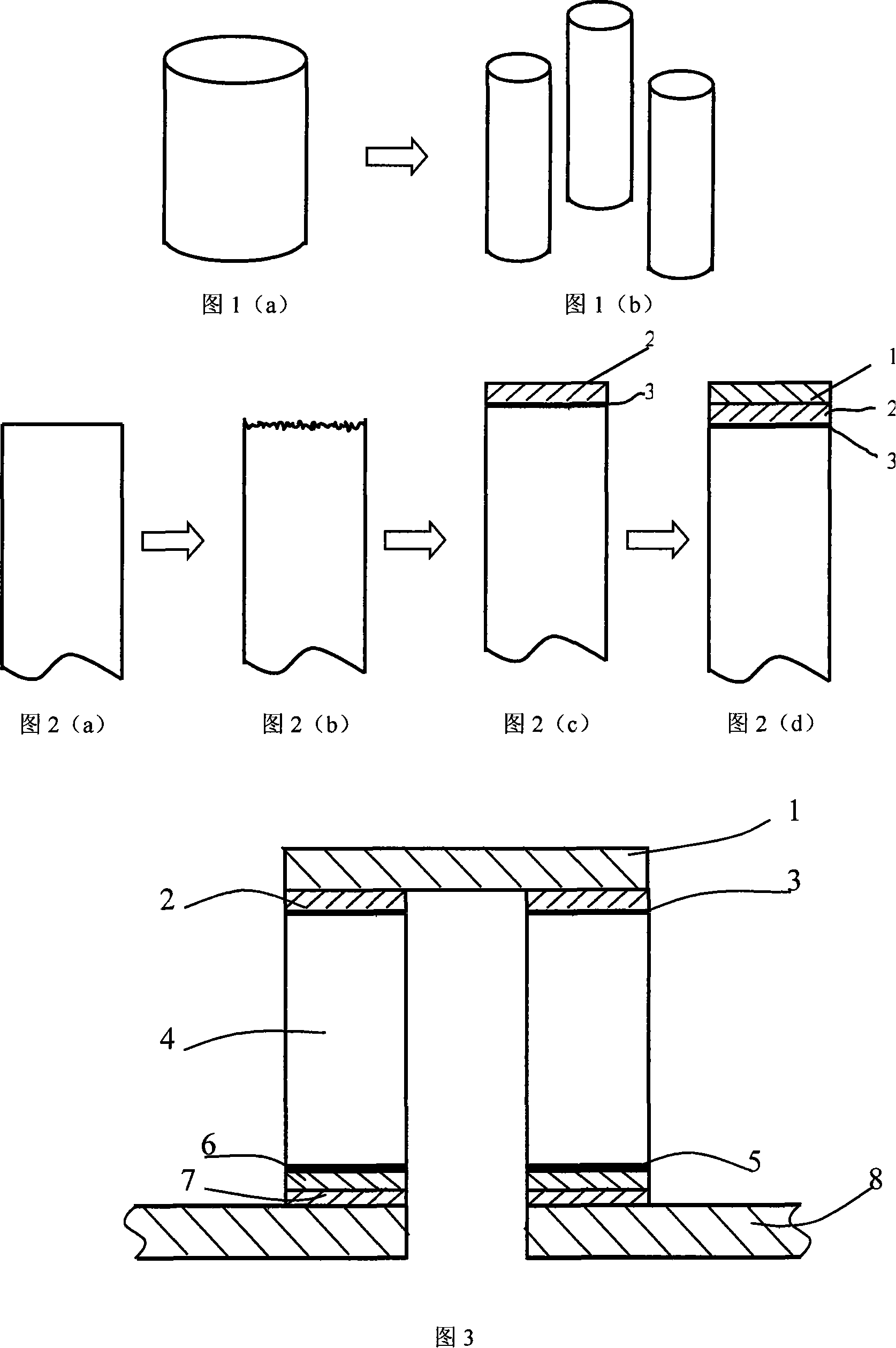
[0028]The cut P-type and N-type thermoelectric pins are first subjected to rough grinding on the two end faces, then ultrasonically cleaned in ethanol, and then plasma sprayed on both ends to form a Mo diffusion barrier layer (3) with a thickness of about 30 μm. Put the P-type and N-type thermoelectric pins (4) into a special mold, put the cut Ag-Cu solder piece (2) and Mo-Cu electrode (1) into the mold in turn on the thermoelectric pins, and perform SPS connection , the sintering pressure is 15MPa, the heating rate is 200°C / min, the temperature is kept at 550°C for 30 seconds, and then the temperature is slowly lowered, and the cooling rate is controlled at 100°C / min, and the welding of the high-temperature end electrode is completed. Put the initially formed π-type device on the Mo diffusion barrier layer (3) at the low temperature end and then vacuum sputter a Ni layer (6) with a thickness of about 20 μm to facilitate better soldering, and then use Sn-Pb solder (7) The low-...
Embodiment 2
[0030] Process and plasma spray the thermoelectric pins that have been cut with the same method and conditions as in Example 1, put P-type and N-type thermoelectric pins (4) into special molds, and place the Ag-Cu soldering pieces that have been cut (2) and Mo-Cu electrode (1) are put into the thermoelectric pin in the mold in turn, and SPS connection is carried out. The sintering pressure is 25MPa, the heating rate is 250°C / min, and the temperature is kept at 550°C for 45 seconds, and then the temperature is slowly lowered. The cooling rate Controlled at 150°C / min, the high-temperature terminal electrode welding is completed. Put the initially formed π-type device on the Mo diffusion barrier layer (3) at the low temperature end and then vacuum sputter a Ni layer (6) with a thickness of about 30 μm to facilitate better soldering, and then use Sn-Pb solder (7) The low-temperature end is soldered to the Cu sheet (8) on the ceramic substrate at a temperature of 180°C. The interf...
Embodiment 3
[0032] The cut thermoelectric legs were treated with the same method and conditions as in Example 1, and then plasma sprayed on both ends to form a W diffusion barrier layer (3) with a thickness of about 20 μm. Put the P-type and N-type thermoelectric pins (4) into a special mold, put the cut Ag-Cu solder piece (2) and Mo-Cu electrode (1) into the mold in turn on the thermoelectric pins, and perform SPS connection , the sintering pressure is 15MPa, the heating rate is 250°C / min, the temperature is kept at 550°C for 60 seconds, and then the temperature is slowly lowered, and the cooling rate is controlled at 100°C / min, and the welding of the high-temperature end electrode is completed. Vacuum sputter a Ni layer (6) with a thickness of about 25 μm on the Mo layer of the low-temperature end of the initially formed π-type device to facilitate better soldering, and then use Sn-Pb solder (7) to connect the low-temperature end to the ceramic The Cu chip (8) on the substrate is connec...
PUM
| Property | Measurement | Unit |
|---|---|---|
| thickness | aaaaa | aaaaa |
| thickness | aaaaa | aaaaa |
| thickness | aaaaa | aaaaa |
Abstract
Description
Claims
Application Information
 - R&D
- Intellectual Property
- Life Sciences
- Materials
- Tech Scout
- Unparalleled Data Quality
- Higher Quality Content
- 60% Fewer Hallucinations
Browse by: Latest US Patents, China's latest patents, Technical Efficacy Thesaurus, Application Domain, Technology Topic, Popular Technical Reports.
© 2025 PatSnap. All rights reserved.Legal|Privacy policy|Modern Slavery Act Transparency Statement|Sitemap|About US| Contact US: help@patsnap.com


