
Three-dimensional slot grid metal semiconductor field effect transistor

A field-effect transistor and metal-semiconductor technology, applied in the field of metal-semiconductor field-effect transistors, can solve problems such as increased short-channel effects and reduced breakdown voltage

Inactive Publication Date: 2007-08-22
UNIV OF ELECTRONICS SCI & TECH OF CHINA
View PDF0 Cites 10 Cited by
  • Summary
  • Abstract
  • Description
  • Claims
  • Application Information

AI Technical Summary

Problems solved by technology

However, the increase of channel doping concentration or channel thickness will reduce the breakdown voltage, while the increase of channel thickness will increase the short channel effect

Method used


Image

  • Three-dimensional slot grid metal semiconductor field effect transistor
  • Three-dimensional slot grid metal semiconductor field effect transistor
  • Three-dimensional slot grid metal semiconductor field effect transistor

Examples


Embodiment Construction

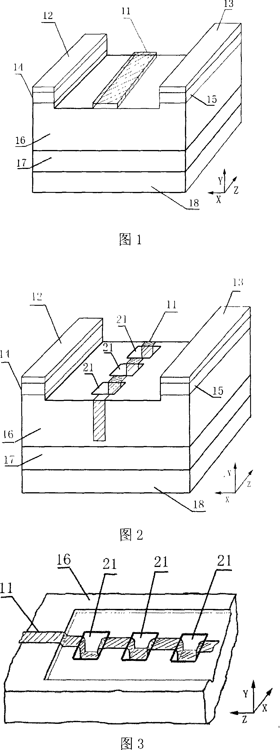
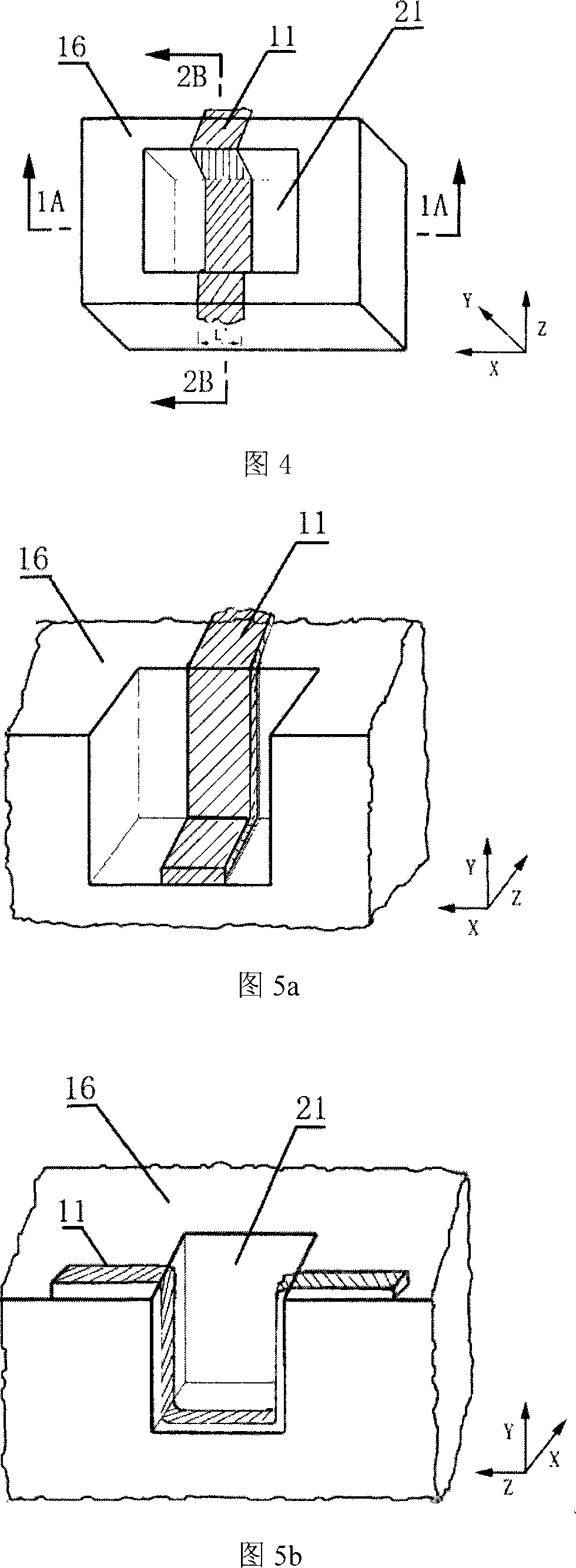
[0031] Three-dimensional trench gate MESFET structure, Fig. 2 is a three-dimensional diagram of the structure proposed by the present invention. It includes: SiC substrate layer 18; p (or n) type buffer layer 17; n (or p) type active layer 16; n (or p) type cap layers 14 and 15; and source electrode 12 and drain electrode 13 . Compared with the traditional MESFET structure, it is characterized in that three (or more) trenches 21 are opened along the Z direction 16 on the active layer, and the gate 11 is covered in the trenches along the Z direction.

[0032] Three-dimensional trench gate MESFET structure, Figure 4 and Figure 5 are schematic diagrams of a single trench structure, which is characterized in that the gate 11 forms a good and continuous contact with the trench sidewall and trench bottom.

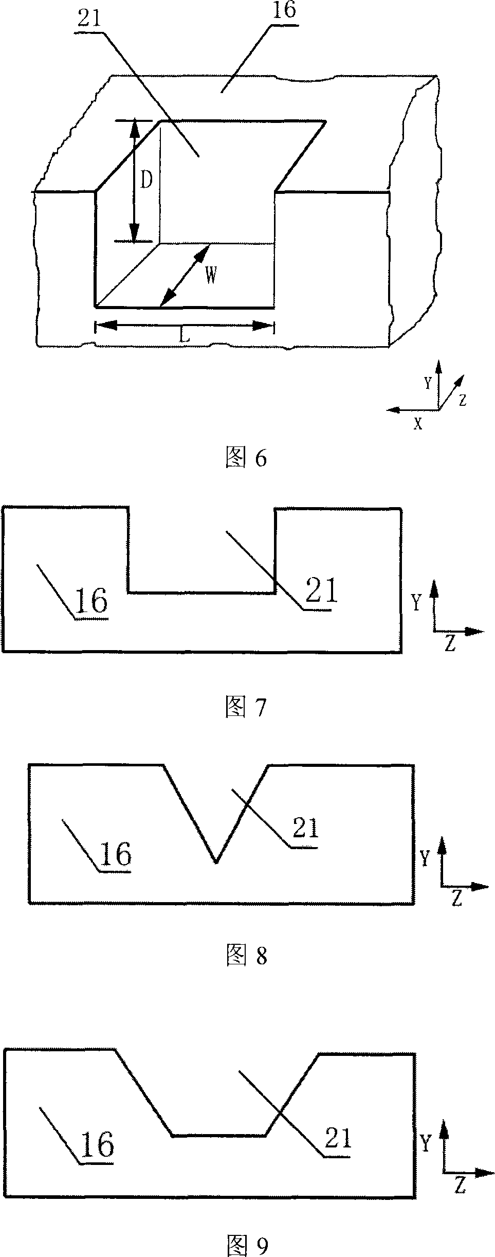
[0033] Compared with the traditional MESFET, the three-dimensional trench gate MESFET structure (Fig. 3) increases the device gate width by n×2D=6D (Fig. 6) where n is the number...


PUM


Abstract

This invention puts forward a kind of 3-D groove grating metal semiconductor field effect transistor structure, which opens one or many grooves in an active layer between the source and drain regions in the shape of a square, V, trapezia or a ladder designed according to the actual needs and the grating electrode is covered in the grooves continuously, which greatly increases grating width in the same surface areas of devices due to the existence of the grating grooves compared with the traditional MESFET structure.

Description

technical field [0001] The present invention relates to a metal semiconductor field effect transistor (Metal-Semiconductor-Field-Effect-Transistor, MESFET), and in particular to such devices with gates formed in trenches. Background technique [0002] In recent years, with the rapid development of microelectronics technology and the urgent needs of aerospace, electronic countermeasures and radar communications and other related fields, the development of new high-frequency and high-power semiconductor devices has attracted more and more attention. Bipolar-Junction-Transistor (BJT) and power Metal-Oxide-Semiconductor Field Effect Transistor (MOSFET) have been widely used in high-power applications. However, BJT is a minority device, which limits its high-frequency application range; compared with MESFET, MOSFET has larger gate capacitance and complicated manufacturing process. The MESFET with a simple manufacturing process can be better applied in the high-frequency field du...

Claims


Application Information

Patent Timeline
Patent Type & Authority Applications(China)
IPC IPC(8): H01L29/423H01L29/772
Inventor 张波张金平邓小川陈壮梁叶毅罗小蓉李肇基
Owner UNIV OF ELECTRONICS SCI & TECH OF CHINA
Learn More