Adhesive film and method for manufacturing semiconductor device using same
A manufacturing method and semiconductor technology, applied in semiconductor/solid-state device manufacturing, semiconductor devices, film/sheet-like adhesives, etc., can solve problems such as peeling problems, and achieve excellent shear strength characteristics and excellent fracture characteristics Effect
- Summary
- Abstract
- Description
- Claims
- Application Information
AI Technical Summary
Problems solved by technology
Method used
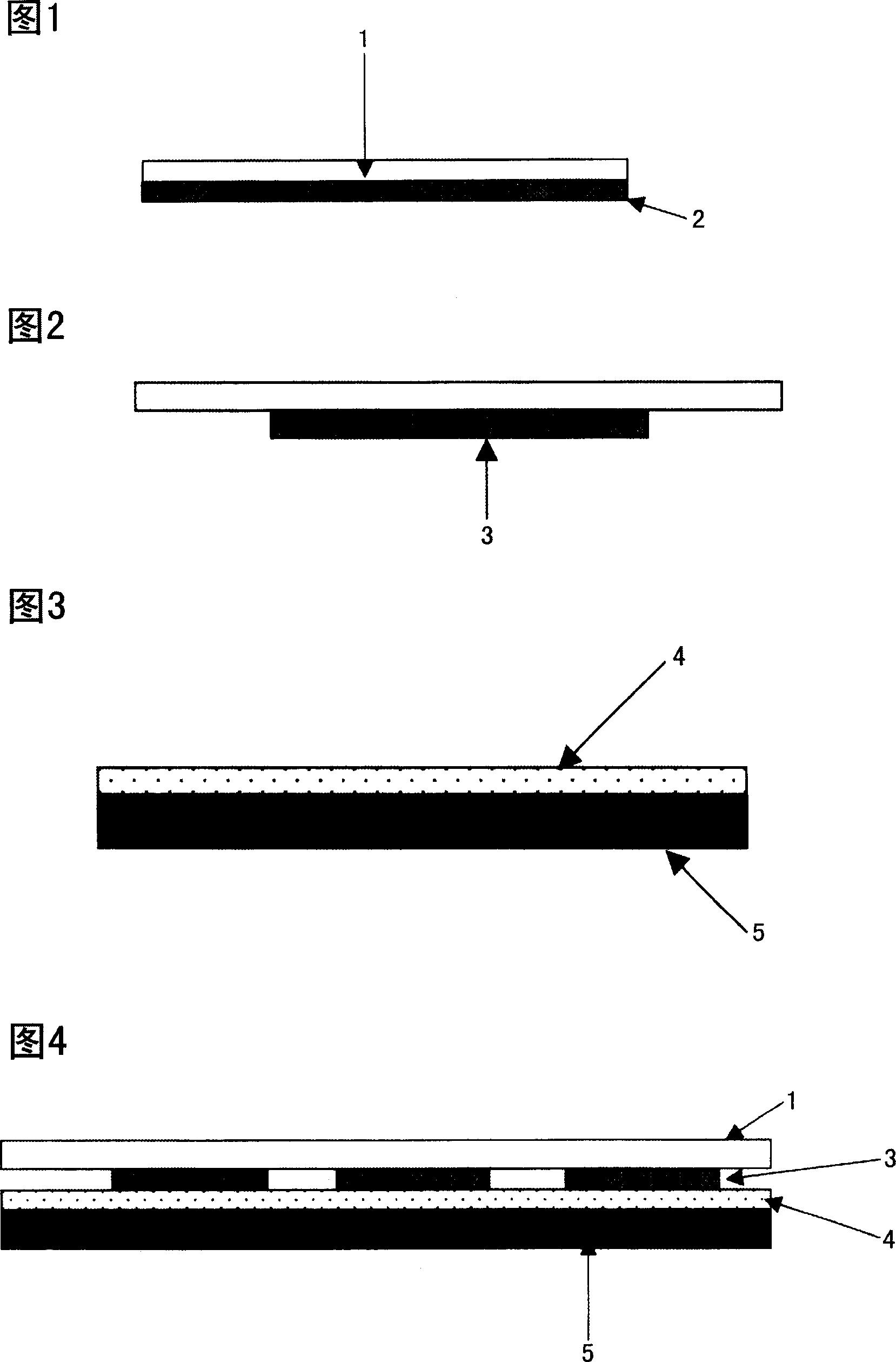
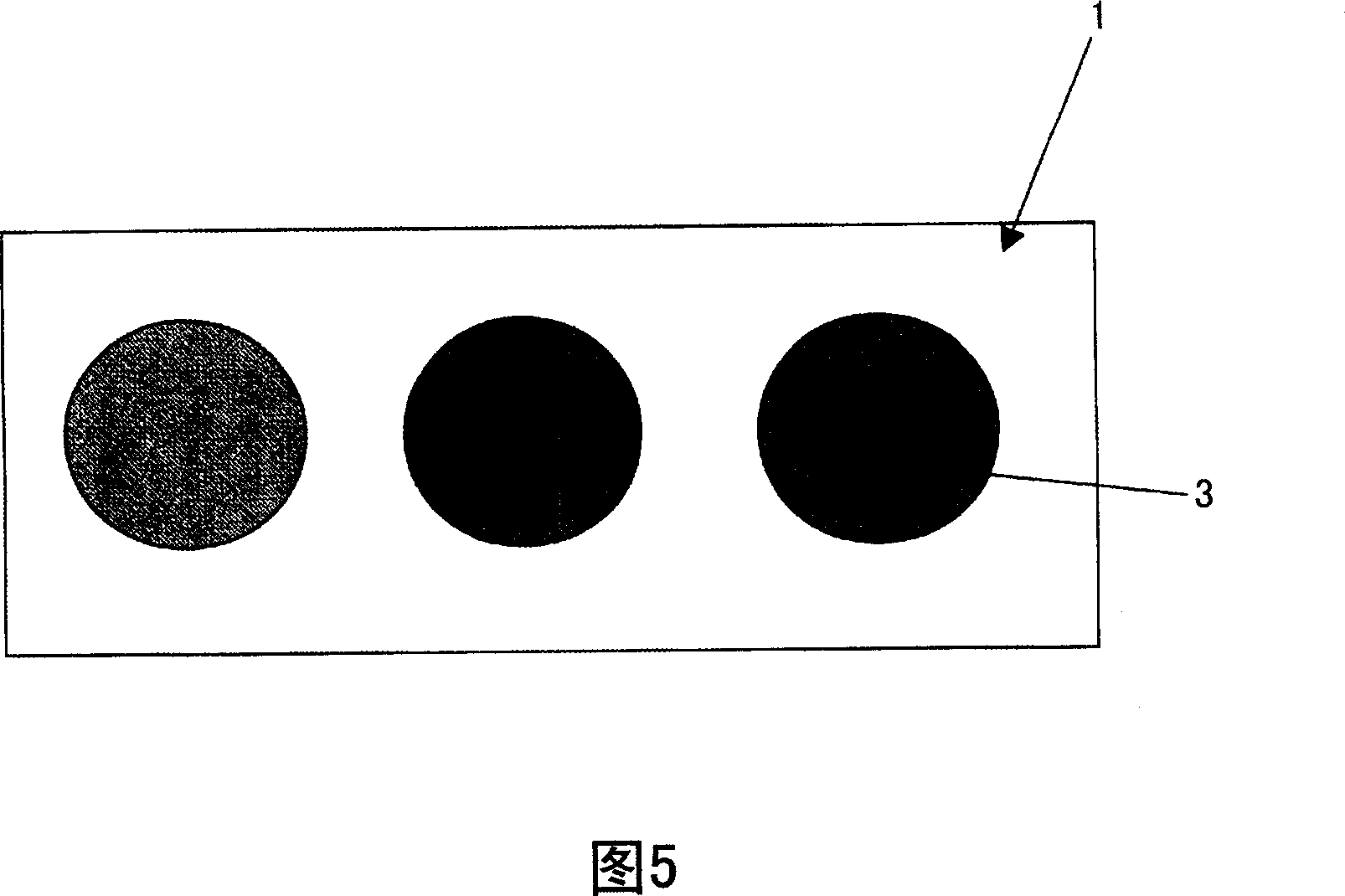
Image

Examples
Embodiment
[0146] Hereinafter, the present invention will be described in further detail through examples, but the present invention is not limited to these examples.
Synthetic example
[0149] (I) Thermosetting adhesive components
[0150] (I-1) Epoxy compound (manufactured by Mitsui Chemicals, Inc., VG3101)
[0151] (I-2) Imidazole-based curing agent (Shikoku Chemical Industry Co., Ltd., 2MAOK-PW)
[0152] (II) Silica-based filler (manufactured by Ryusen Co., Ltd., 1-FX)
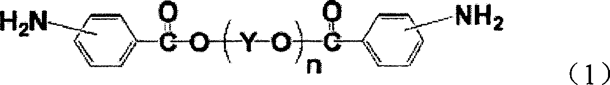
[0153] (III) Synthesis example of polyimide resin component
Synthetic example 1
[0155] In a 30 ml five-necked separable flask with a stirrer, a nitrogen inlet tube, a thermometer, and a Dean Stark tube filled with mesitylene, quantitatively add 4,4′-bis(3 -aminophenoxy)biphenyl 17.00g, polytetrahydrofuran-di-p-aminobenzoate (manufactured by Ihara Chemical Industry Co., Ltd., trade name: Erasma-1000, average molecular weight 1305) 40.14g, N-methyl- 86.37 g of 2-pyrrolidone and 37.09 g of mesitylene were heated to 50° C. in a nitrogen atmosphere to dissolve them, and then 25.05 g of oxy-4,4′-diphthalic dianhydride was gradually added in small amounts. Then, a nitrogen gas introduction tube was inserted (foaming state), and the temperature in the system was heated to 170° C. to 180° C. to azeotropically remove water while maintaining it for 10 hours. After cooling, 61.67 g of N-methyl-2-pyrrolidone and 26.49 g of mesitylene were added and diluted to obtain a solution of polyimide (III-1). After making a solution in N-methyl-2-pyrrolidone with a concentratio...
PUM
| Property | Measurement | Unit |
|---|---|---|
| peel strength | aaaaa | aaaaa |
| glass transition temperature | aaaaa | aaaaa |
| glass transition temperature | aaaaa | aaaaa |
Abstract
Description
Claims
Application Information
 - R&D
- Intellectual Property
- Life Sciences
- Materials
- Tech Scout
- Unparalleled Data Quality
- Higher Quality Content
- 60% Fewer Hallucinations
Browse by: Latest US Patents, China's latest patents, Technical Efficacy Thesaurus, Application Domain, Technology Topic, Popular Technical Reports.
© 2025 PatSnap. All rights reserved.Legal|Privacy policy|Modern Slavery Act Transparency Statement|Sitemap|About US| Contact US: help@patsnap.com