
Preparation process of nanometer monocrystalline zinc oxide film material

A nano-film material, zinc oxide single crystal technology, applied in the field of optoelectronic materials, can solve the problems of complex equipment and process, high cost, and achieve the effect of reducing injection cost, good quality and good insulation

Inactive Publication Date: 2009-10-07
WUHAN UNIV
View PDF1 Cites 0 Cited by
  • Summary
  • Abstract
  • Description
  • Claims
  • Application Information

AI Technical Summary

Problems solved by technology

[0004] The purpose of the invention is to overcome the shortcomings of complex equipment and high cost in the preparation of zinc oxide film materials in the prior art, and provide a method for preparing zinc oxide single crystal nano-films with simple equipment and process and low cost, and High quality ZnO single crystal nano film can be obtained by this method

Method used


Image

  • Preparation process of nanometer monocrystalline zinc oxide film material
  • Preparation process of nanometer monocrystalline zinc oxide film material

Examples


Embodiment 1

[0016] Zn with an energy of 200keV + Injected into quartz glass, the injection dose is 2×10 17 ions / cm 2 .

[0017] The injected sample was annealed in the air at 750°C for 1 hour in an ordinary annealing furnace, and the heating rate was 20°C / min. When the temperature reached 700°C, the Zn atoms in the sample gradually evaporated to the surface of the sample and reacted with oxygen in the air. ZnO is formed on the surface. Incubate at 750°C for 1 hour so that all the Zn atoms in the substrate evaporate to the surface of the substrate. Cool down naturally after annealing.

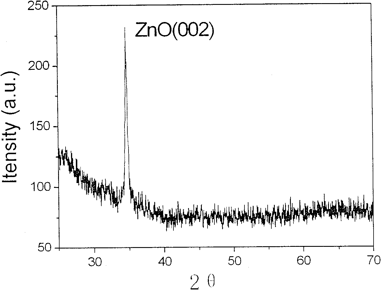
[0018] Analyze the sample prepared in this embodiment, figure 1 It is the X-ray diffraction (XRD) curve of the zinc oxide single crystal nano film prepared by this example, only (002) plane diffraction peak is shown in the figure, shows that the film grows along the c-axis direction, and has very high quality.

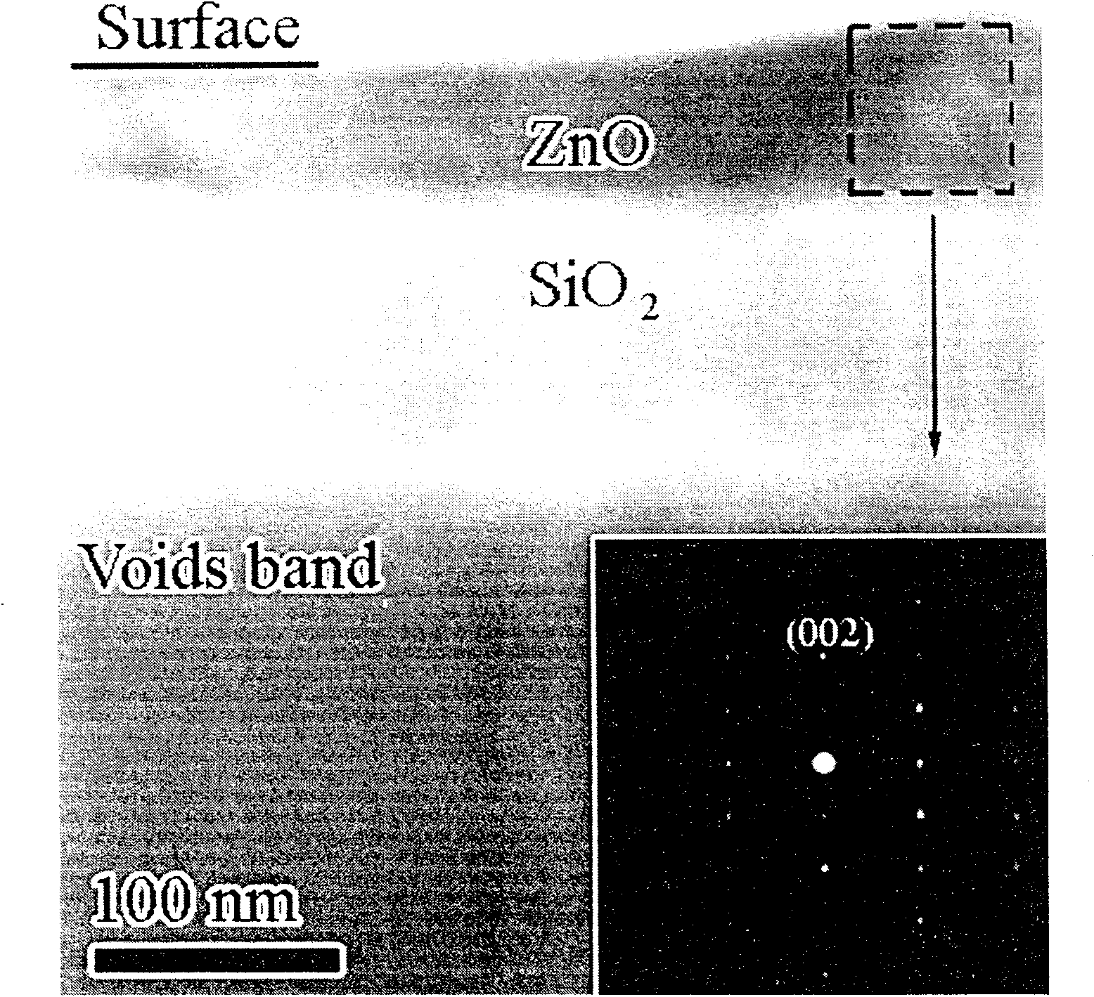
[0019] figure 2 It is the transmission electron microscope (TEM) cross-sectional image a...

Embodiment 2

[0021] Zn with an energy of 50keV + Inject into quartz glass with MEVVA source implanter, the injection dose is 3×10 17 ions / cm 2 .

[0022] The injected sample was annealed in the air at 700°C for 2 hours in a common annealing furnace, and the heating rate was 10°C / min. When the temperature reached 700°C, the Zn atoms in the sample gradually evaporated to the surface of the sample and reacted with oxygen in the air. ZnO is formed on the surface. Keep the temperature at 700°C for 2 hours so that all the Zn atoms in the substrate evaporate to the surface of the substrate. Cool down naturally after annealing.

[0023] The sample prepared in this embodiment was analyzed, and the X-ray diffraction (XRD) curve and transmission electron microscope (TEM) cross-sectional image of the sample also proved that a ZnO single crystal nano film was formed.


PUM


Abstract

The invention provides a preparation method of zinc oxide single crystal nano film material. The method adopts the method of heat treatment after zinc ion implantation to form a ZnO single crystal nano film on the surface of the material. The specific steps included are as follows: first implant Zn+ with an energy of 50 to 300keV into the quartz glass, and then place it in the air Annealing, the annealing temperature is 700-750°C, the annealing time is 1-2 hours, and the heating rate is 10-20°C / min. The Zn atoms injected into the quartz glass gradually evaporated to the surface of the sample and oxidized on the surface to form a ZnO single crystal nano-film. The invention has the characteristics of simple preparation method, low cost and high quality of the obtained single crystal thin film, and thus can be widely used in the field of optoelectronics.

Description

technical field [0001] The invention relates to a preparation method of a novel semiconductor nanometer thin film material, in particular to a preparation method of a zinc oxide single crystal thin film material, belonging to the technical field of optoelectronic materials. Background technique [0002] ZnO is a new type II-VI wide bandgap compound semiconductor material with a hexagonal structure. Its room temperature bandgap is about 3.37eV, and the exciton binding energy is as high as 60meV. It is used in various light-emitting devices such as ultraviolet light, blue light, and blue-green light. In 1997, Nature Magazine spoke highly of the application prospects of lasers made of ZnO in improving optical storage. The band-edge emission of ZnO is very suitable as an excitation light source material for white LEDs in the ultraviolet region, which highlights the important position of ZnO in semiconductor lighting engineering. At the same time, due to the good light transmis...

Claims


Application Information

Patent Timeline
Patent Type & Authority Patents(China)
IPC IPC(8): C30B29/16C30B29/64
Inventor 任峰蒋昌忠
Owner WUHAN UNIV
Learn More