Wiring substrate of a semiconductor component comprising external contact pads for external contacts and method for producing the same

A technology for wiring substrates and contact pads, applied in semiconductor/solid-state device components, semiconductor devices, electric solid-state devices, etc., can solve problems such as being unsuitable for mass production, concentration, and complex costs

Inactive Publication Date: 2009-08-19
INFINEON TECH AG
View PDF8 Cites 0 Cited by
  • Summary
  • Abstract
  • Description
  • Claims
  • Application Information

AI Technical Summary

Problems solved by technology

Based on the specific military application, this type of so-called "floating pad" solder ball requires a more complex and cost-intensive manufacturing method and is therefore also not suitable for mass production

Method used


Image

  • Wiring substrate of a semiconductor component comprising external contact pads for external contacts and method for producing the same
  • Wiring substrate of a semiconductor component comprising external contact pads for external contacts and method for producing the same
  • Wiring substrate of a semiconductor component comprising external contact pads for external contacts and method for producing the same

Examples


Embodiment Construction

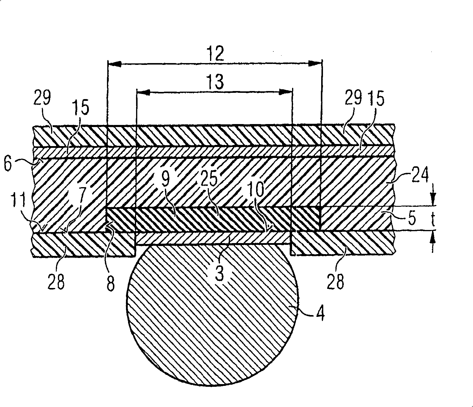
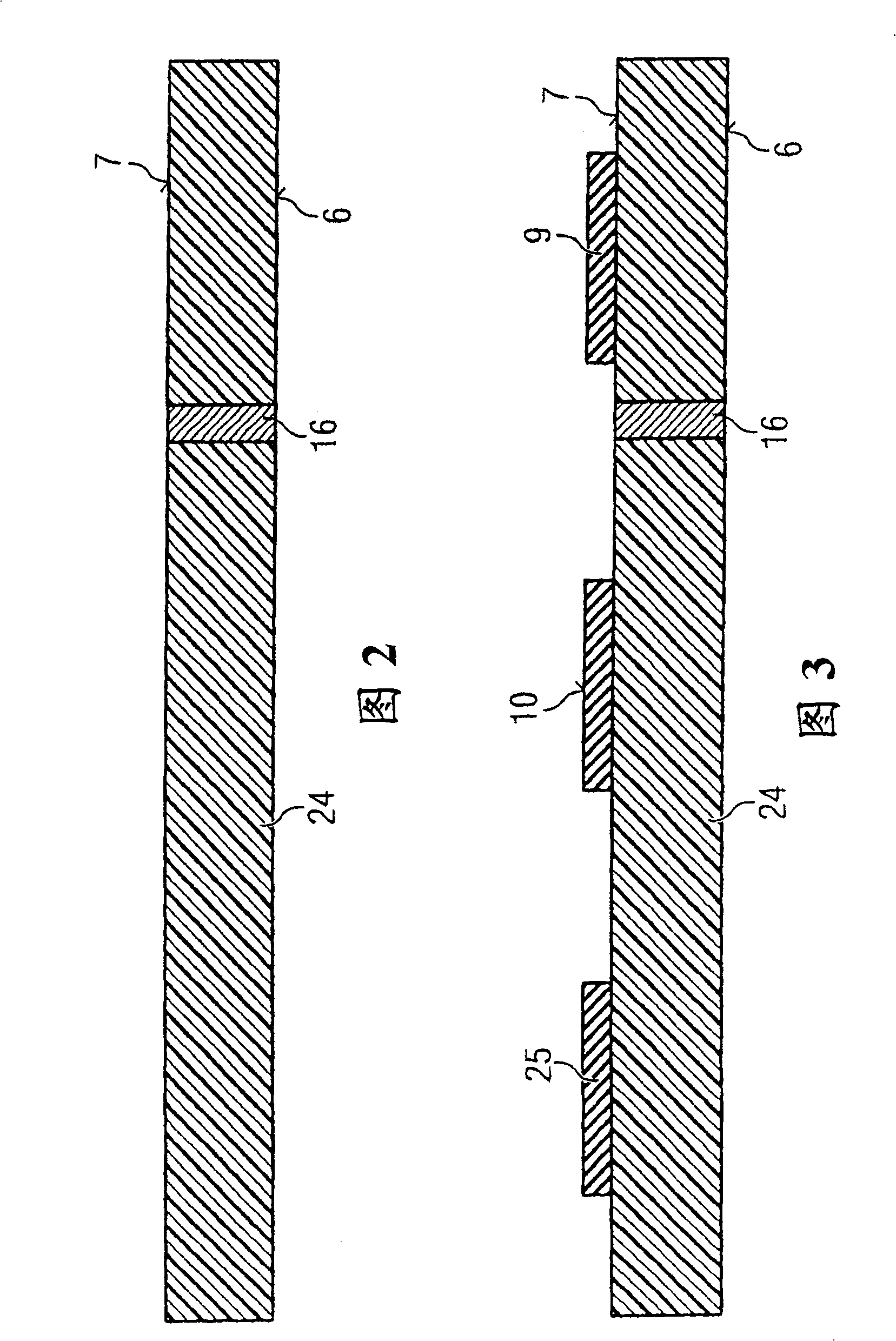
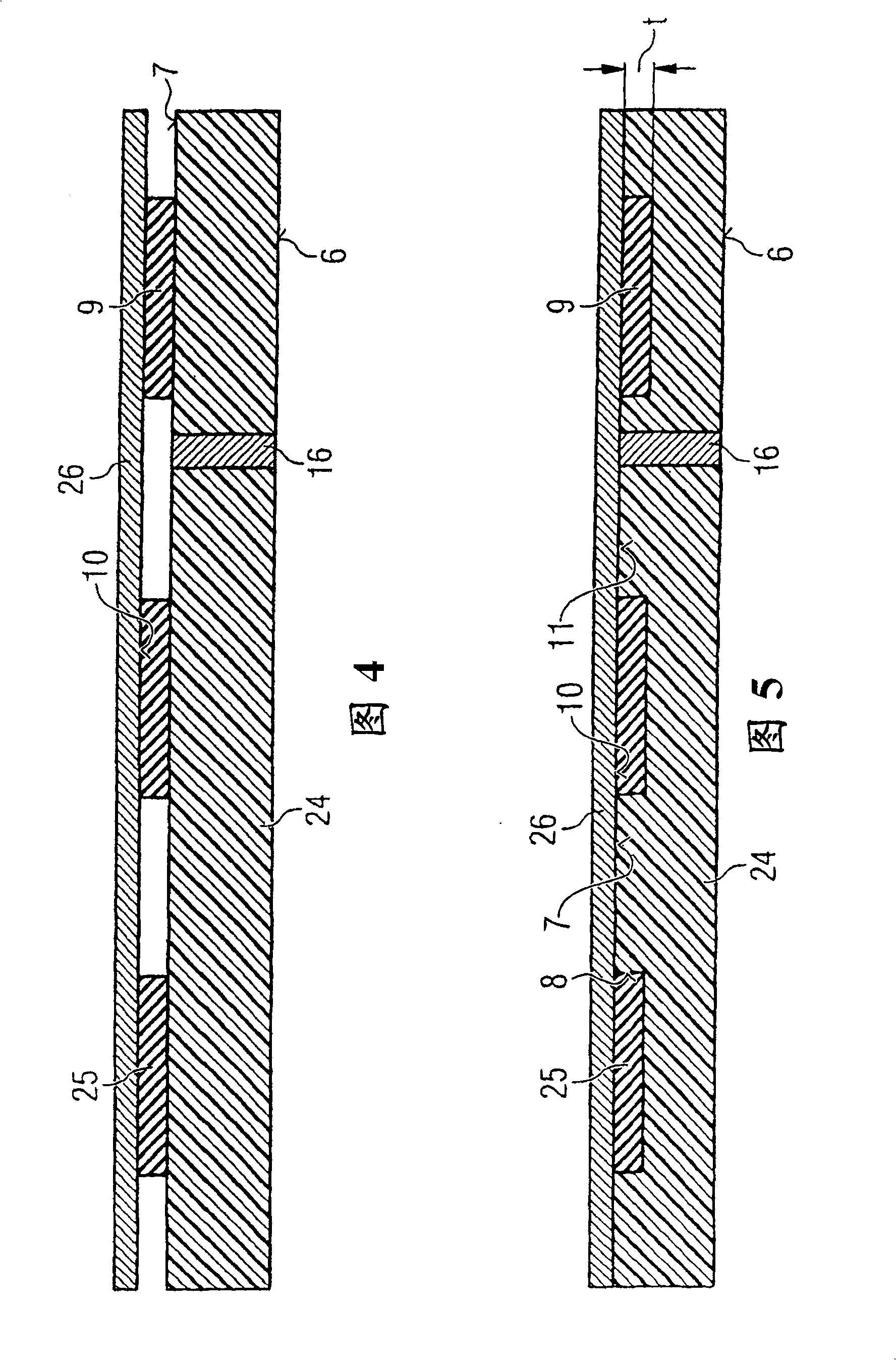
[0051] figure 1 Shown is a schematic cross-sectional view through a part of the wiring substrate 5 . The wiring substrate 5 has a base plate 24 with a top side 7 and a bottom side 6 . From the top side 7 an elastic material 9 is introduced into the substrate 24 , which material forms an elastic material spacer 25 and fills the cutout 8 on the top side 7 of the wiring substrate 5 .

[0052] The spacer 25 of elastomeric material incorporated into the substrate 24 has a top side 10 forming a coplanar area 11 with the top side 7 of the wiring substrate 5 . The metallic external contact pads 3 are arranged on the coplanar area 11 of the wiring substrate 5 in the region of the pad 25 of elastomeric material. The area extent 13 of the outer contact pad 3 is smaller than the area extent 12 of the elastomeric pad 25 .

[0053] Because the elastomeric pad 25 is compliant, shear loads due to thermal stress or vibration loads acting on the external contact pad 3 can be reduced or dampe...


PUM


Abstract

The invention relates to a wiring substrate (5) of a semiconductor component (3) comprising external contact pads (3) for external contacts of the semiconductor component. For this purpose, the rigid wiring substrate (5) has a top side (7) with a cutout (8), wherein the cutout (8) has a highly elastic material (9). External contact pads (3) are arranged on the high elastic material (9). Furthermore, the invention relates to a method for manufacturing a wiring substrate (5) of this type, wherein during the manufacturing method a spacer of elastomeric material (25) is pressed into a precursor of polymer plastic.

Description

technical field [0001] The present invention relates to a wiring substrate of a semiconductor component including external contact pads for external contacts and a method of manufacturing the same. In this case, solder balls are preferably applied as external contacts to the external contact pads. Background technique [0002] This type of wiring substrate is used for housings of semiconductor components, which are also called BGA housings (Ball Grid Arrays) or LBGA housings (Large Ball Grid Arrays). [0003] One of the problems with said wiring substrate is the reliability of the connection between the external contact pads of the wiring substrate and the super circuit board which can thus be produced. During a cyclic thermal load event, a cyclic mechanical shear load is applied to the solder connection due to the presence of different materials with different coefficients of thermal expansion. In a shock loading event, in addition to the shear load of cyclic thermal stre...

Claims


Application Information

Patent Timeline
Patent Type & Authority Patents(China)
IPC IPC(8): H01L23/498H05K1/02H01L23/00H05K3/32
CPCH01L23/562H05K1/114H01L23/49816H01L24/48H01L2224/48465H05K2201/091H05K2201/0355H01L2224/16H05K2203/0278H01L23/49811H01L2224/48227H05K1/0271H05K2201/0133H05K2201/0187H01L2924/15311H01L2924/01029H01L2224/16225H01L2224/48091H01L2224/73265H01L2924/01013H05K1/111H01L2224/32225H01L24/73H01L2224/0557H01L2224/05573H01L2924/00014H01L2924/181H01L2924/15173H01L2224/16237H01L2224/05571H01L2224/0554Y02P70/50H01L2924/00012H01L2924/00H01L2224/05599H01L2224/45099H01L2224/45015H01L2924/207H01L2224/0555H01L2224/0556H01L23/50
Inventor M·鲍尔R·斯泰纳H·沃纳
Owner INFINEON TECH AG
Why Eureka
Try Eureka