Film stress detecting method
A stress detection and film layer technology, applied in the field of integrated circuit manufacturing, can solve the problem of difficulty in achieving accurate thickness measurement in the selected area of the sample, and achieve the effects of reducing waste chip loss, expanding the process range and reducing production costs.
- Summary
- Abstract
- Description
- Claims
- Application Information
AI Technical Summary
Problems solved by technology
Method used
Image

Examples
no. 2 example
[0051] As a second embodiment of the present invention, the specific steps of applying the method of the present invention to detect film stress include:
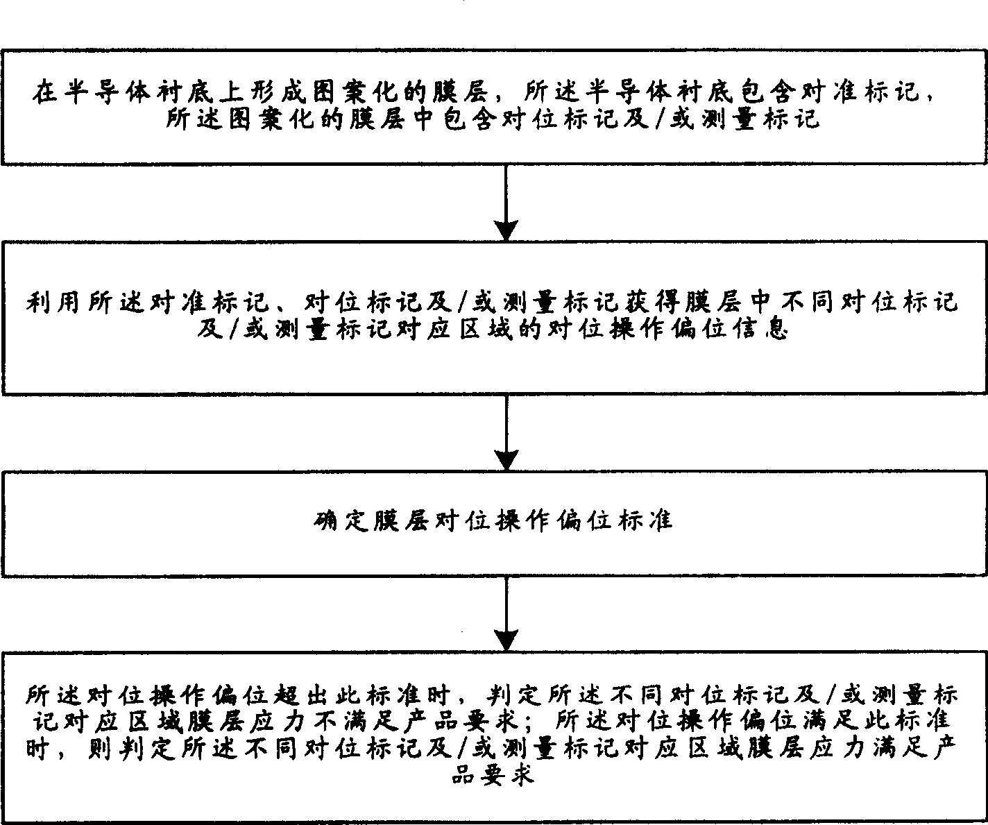
[0052] First, film deposition-photolithography-etching steps are performed on a semiconductor substrate to obtain a patterned film layer.
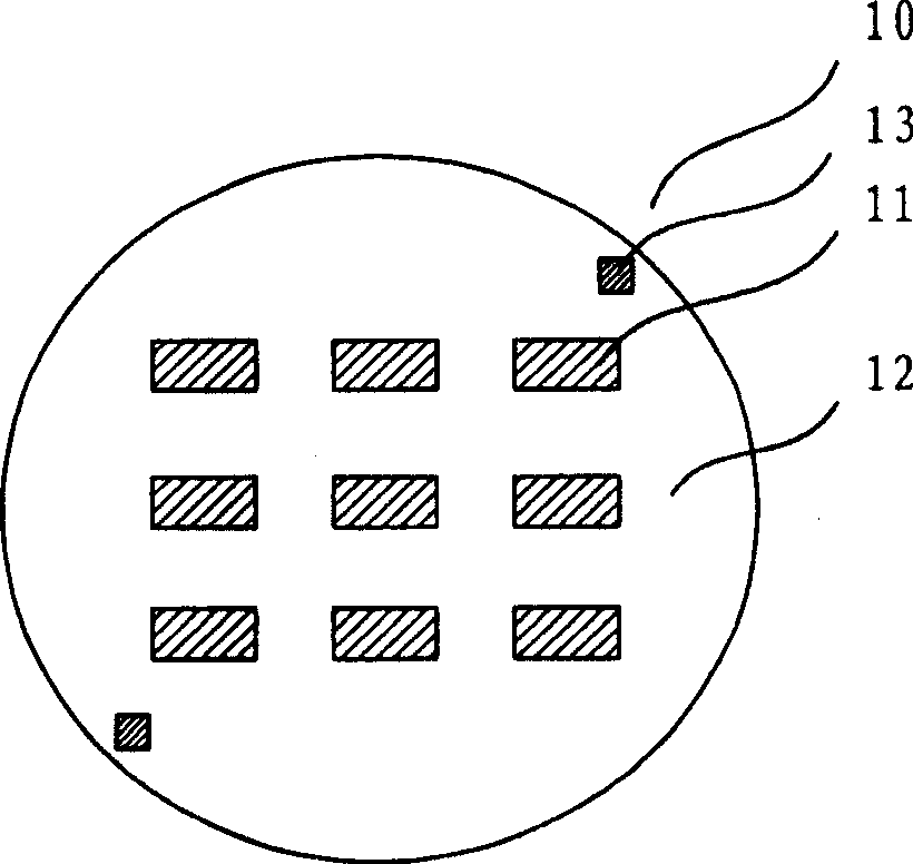
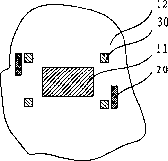
[0053] The semiconductor substrate includes a graphic area and a non-graphical area, the graphic area is used to make device products, and the non-graphical area is used to undertake various marks needed in the actual production process, such as alignment marks and measurement Marking, etc., and provide cutting channels after the device is completed. Alignment marks are included in the non-pattern area of the semiconductor substrate. The alignment mark is used to provide an alignment point located in the non-pattern area of the semiconductor substrate required for an alignment operation by using the exposure device to form a patterned film layer. As a second embodiment of the pres...
PUM
 Abstract
Description
Claims
Application Information
 - Generate Ideas
- Intellectual Property
- Life Sciences
- Materials
- Tech Scout
- Unparalleled Data Quality
- Higher Quality Content
- 60% Fewer Hallucinations
Browse by: Latest US Patents, China's latest patents, Technical Efficacy Thesaurus, Application Domain, Technology Topic, Popular Technical Reports.
© 2025 PatSnap. All rights reserved.Legal|Privacy policy|Modern Slavery Act Transparency Statement|Sitemap|About US| Contact US: help@patsnap.com