
Polar envelope correction mechanism for enhancing linearity of RF/microwave power amplifier

a technology of linearity and correction mechanism, applied in the field of communication systems, can solve the problems of inapplicability of baseband correction techniques using baseband signals, inability to achieve practical solutions for correcting distortion, and inability to use conventional correction mechanisms such as feed forward or predistortion schemes, etc., to achieve the effect of improving linearity of non-linear microwave/rf power amplifiers, simple, efficient and effective, and reducing the bandwidth of digital modulation

Inactive Publication Date: 2001-10-16
INTEL CORP
View PDF33 Cites 69 Cited by
  • Summary
  • Abstract
  • Description
  • Claims
  • Application Information

AI Technical Summary

Benefits of technology

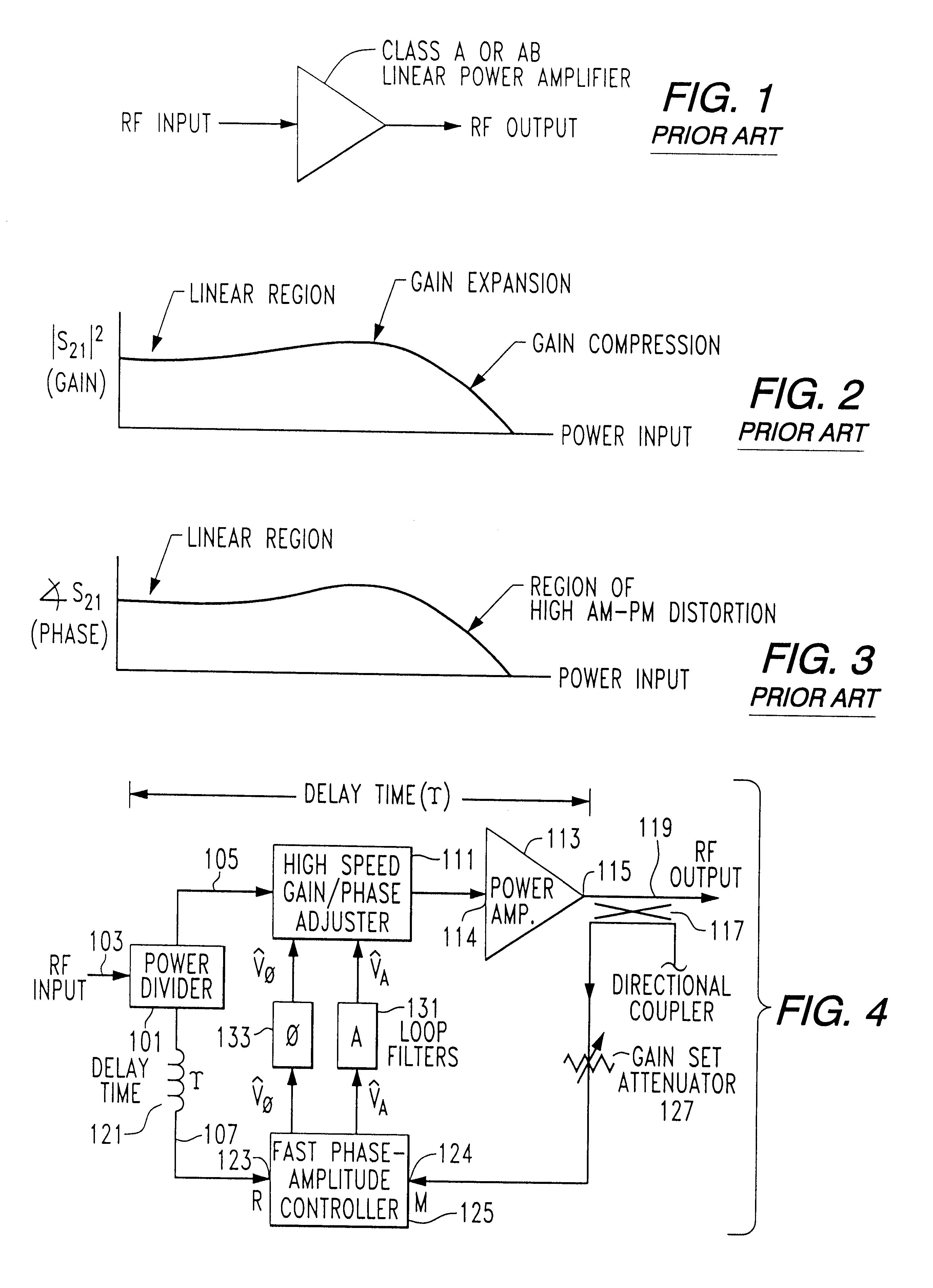
The present invention takes advantage of the relatively modest bandwidth of digital modulation formats such as those shown in Table 1, by providing an amplitude and phase distortion correction strategy that is based upon signal envelope feedback. In particular, the present invention provides a simple, yet efficient and effective way of improving the linearity of a non-linear microwave / RF power amplifier employed for digital modulation formats having signal bandwidths in the KHz to low MHz range, through the use of a polar envelope-responsive correction (PEC) mechanism, which operates directly on the RF signal passing through the power amplifier, requires no baseband information, and reduces the AM-to-PM and AM-to-AM distortion which causes spectral regrowth of digital modulation formats such as TDMA, CDMA and GSM. The correction mechanism of the invention enables the power amplifier to comply with linearity and spectral regrowth requirements imposed by both government regulatory agencies (such as the Federal Communications Commission (FCC)) and industry standards.
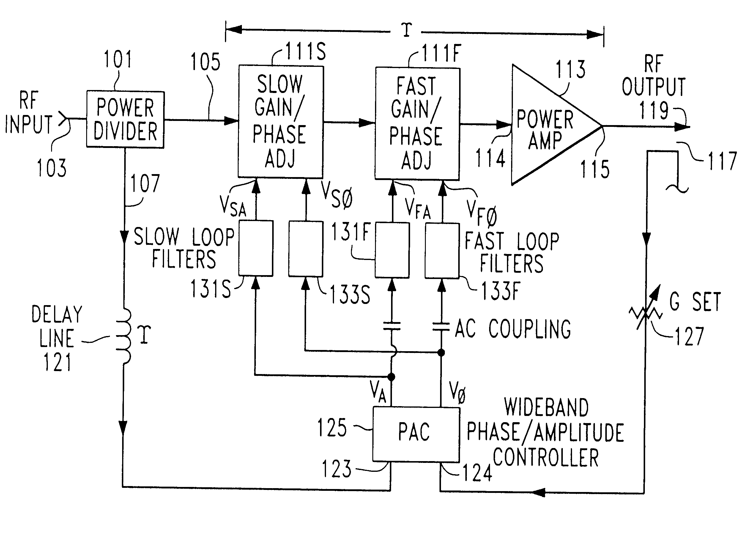
A delay line is usually installed in the reference path to reduce phase differences between the main and reference paths which arise from the larger delay of the main path. This ensures that the main and reference path signals arrive at the phase amplitude controller at the same time.
In order to maintain stability, the inverse of the time delay (1 / t) through the feedback path is greater than the bandwidth occupied by the envelope of the signal being processed. The amplitude control loop and the phase control loop interact minimally with one another and have adequate bandwidth to process all of the frequency components contained in the spectrum of the input signal envelope. The response of both of the gain and phase control loops is such that each loop has adequate gain and phase margin to prevent instability and unacceptable transient behavior.
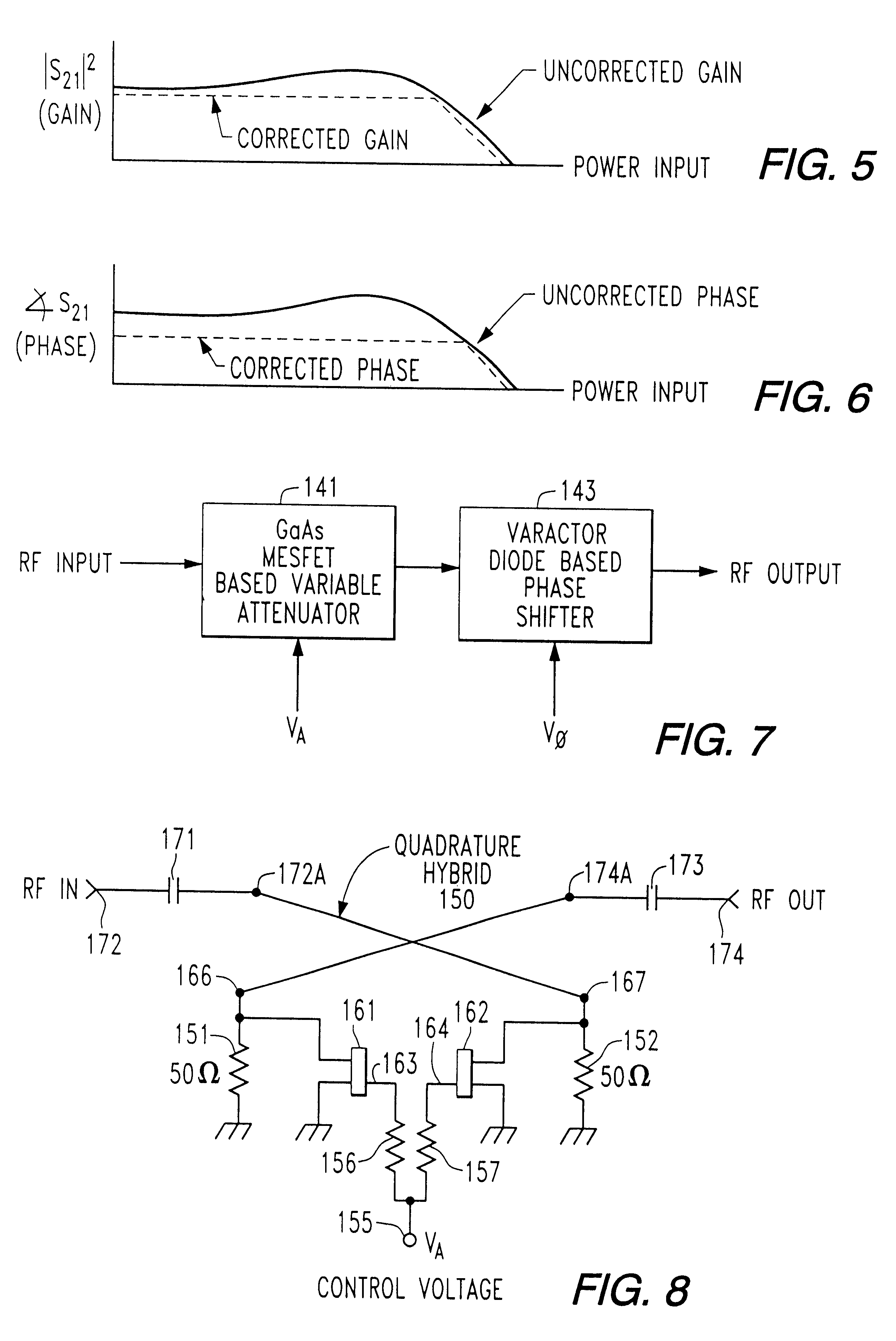
When the control input voltage V.sub.A to each MESFET is biased at a first DC voltage value (e.g. -5V), current flow through the MESFETs' source-drain paths is cut off, so that the MESFETs are rendered non-conductive or placed in the high impedance state. As a result, all of the RF energy delivered to the input of the fast variable attenuator and the quadrature hybrid attenuator will be absorbed by the MESFET's parallel 50 ohm resistors, thereby providing maximum attenuation. As the control voltage V.sub.A applied to the MESFET gate terminals is increased (e.g., from -5V toward zero volts), the effective resistance of the MESFETs and their parallel resistors decreases, since the parallel resistors become shunted by the monotonically decreasing resistance of the MESFETs, whereby more and more RF energy is reflected to the fast variable attenuator's RF output port.
For this purpose, the gain / phase adjuster in the main signal path is implemented as a slow gain / phase adjuster, connected in cascade with a fast gain / phase adjuster. The control voltages V.sub.A and V.sub..PHI. generated by the phase / amplitude controller for the two gain / phase adjusters are coupled through respective slow and fast pair of loop filters. Such separate loops not only reduce the slew rate requirements imposed on loop components but also reduce the amount of the range of the amplitude and phase adjuster that must be traversed at fast rates. As a result, the relatively slow and fast loops can be centered in an optimal portion of the control component's (variable attenuator, phase shifter, vector modulator) operating curve. This greatly eases the task of obtaining stable, wide bandwidth control loops. Namely, dividing each loop into a relatively fast loop that tracks the modulation envelope of the signal incident on the RF amplifier, and a relatively slow loop that tracks only environmentally induced changes facilitates the design of stable wideband polar envelope correction loops.

Problems solved by technology

Unfortunately, conventional correction mechanisms, such as feed forward or predistortion schemes, are complex, inefficient, and prohibitively expensive to be practical solutions for correcting distortion in the majority of single carrier linear power amplifiers.
Since baseband I and Q data is usually not available at the power amplifier, baseband correction techniques which make use of baseband signals, such as baseband cartesian feedback, are also not applicable.

Method used


Image

  • Polar envelope correction mechanism for enhancing linearity of RF/microwave power amplifier
  • Polar envelope correction mechanism for enhancing linearity of RF/microwave power amplifier
  • Polar envelope correction mechanism for enhancing linearity of RF/microwave power amplifier

Examples


first embodiment

FIG. 17 schematically illustrates a circuit implementation of the high speed phase / amplitude controller 125 of FIG. 4, configured as a differential peak detector 240 for envelope amplitude comparison and a phase bridge 250 serving as a phase detector. In the differential peak detector 240, input signals are coupled to respective R (reference) and M (measure) input ports 123 and 124 through respective dc blocking capacitors 245 and 246, resistors 251 and 253 and peak detector diodes 255 and 256 to (-) and (+) input ports 257 and 258 of differential amplifier 260. The (+) and (-) input ports 257 and 258 of differential amplifier 260 are further coupled through respective capacitors 265 and 266 and resistors 271 and 273 to ground. Isolation resistors 251 and 253, detector diodes 255 and 256, by-pass capacitors 265, 266 and video load resistors 271 and 273 comprise a pair of fast biased peak detectors which measure the amplitude of the envelopes of the signals delivered to the R and M p...

second embodiment

FIG. 18 schematically illustrates a circuit implementation of the high speed phase / amplitude controller 125 of FIG. 4, configured with peak detectors and a Gilbert multiplier. In the embodiment of FIG. 18, the R and M input terminals 123 and 124, respectively, are each split into two paths by quadrature power divider 311 and in phase power divider 312. The in phase R paths and one of the M paths are each peak detected by means of a pair of matched, biased diode detectors 321 and 322, respectively, and coupled to (+) and (-) inputs 331 and 332 of differential amplifier 330. The output of differential amplifier 330 is the control voltage V.sub.A.

The control voltage V.sub..PHI. is obtained by multiplying the remaining quadrature R and in phase M signals limited by respective phase-matched limiters 341 and 343 in a wideband Gilbert cell multiplier 350 and low pass filtering the result by means of a low pass filter 352. The phase matched limiters 341 and 343 remove amplitude information ...


PUM


Abstract

Linearity of an RF / microwave power amplifier is enhanced by an amplitude and phase distortion correction mechanism based upon signal envelope feedback, that operates directly on the RF signal passing through the power amplifier. A phase-amplitude controller responds to changes in gain and phase through the RF / microwave power amplifier signal path caused by changes in RF input power, DC power supply voltages, time, temperature and other variables, and controls the operation of a gain and phase adjustment circuit, so as to maintain constant gain and transmission phase through the RF / microwave power amplifier.

Description

FIELD OF THE INVENTIONThe present invention relates in general to communication systems, and is particularly directed to a polar envelope responsive correction mechanism for reducing amplitude and phase distortion in a microwave and RF power amplifier that is designed to amplify signals whose bandwidth is in the KHz to low MHz spectral range.BACKGROUND OF THE INVENTIONAs the wireless communications market continues to expand, the accompanying need for increased capacity is forcing a move from analog modulation techniques, such as frequency modulation (FM), to digital modulation formats, such as time division multiple access (TDMA) and code division multiple access (CDMA), which have bandwidths listed in Table 1.TABLE 1 US DAMPs (TDMA) 30 kHz GSM 277 kHz CDMA 1.23 MHzBoth TDMA and CDMA modulation require somewhat greater linearity than can be routinely obtained in an uncorrected, high efficiency class AB power amplifier. Unfortunately, conventional correction mechanisms, such as feed...

Claims


Application Information

Patent Timeline
IPC IPC(8): H03F1/32H03G1/00
CPCH03F1/3247H03F1/3282H03F2200/438H03F2200/57H03G1/0064H03G1/007H03F1/32
Inventor EISENBERG, JOHN A.BASKIN, BRIAN L.ROBERTSON, III, CHARLES STUARTSTATEZNI, DIETER WERNERMUCENIEKS, LANCE TODDBRUBAKER, DAVID LEE
Owner INTEL CORP
Learn More