
Systems for nonlinear optical wave-mixing

a nonlinear, optical wave-mixing technology, applied in the field of optics, can solve the problems of not all materials can benefit from the waveguide-based phase-matching technique outlined, the dispersion-engineered geometry of the waveguide does not meet the fabrication constraints of multi-project-wafer-oriented silicon photonics, and the development of silicon-based converters is often not compa

Inactive Publication Date: 2018-03-13
VRIJE UNIV BRUSSEL
View PDF12 Cites 1 Cited by
  • Summary
  • Abstract
  • Description
  • Claims
  • Application Information

AI Technical Summary

Benefits of technology

The patent aims to provide better methods and systems for mixing nonlinear optical waves, such as SFG, DFG, and FWM (e.g. Raman-resonant FWM and Kerr-induced FWM). The invention's advantages include efficient mixing at suitable wavelengths for use in telecommunication and spectroscopy.

Problems solved by technology

First of all, not all materials used for SFG, DFG, Raman-resonant or Kerr-induced FWM are as easily workable as silicon to fabricate waveguide structures, which implies that not all materials can benefit from the waveguide-based phase-matching technique outlined above.
Furthermore, even if one considers only a material such as silicon for which the waveguide-based phase-matching technique described above is well developed, it is important to know that, although the phase-matching bandwidth of the silicon nanowire referred to above is more than wide enough to enable phase-matched Raman-resonant FWM in the near-infrared at a pump-signal frequency shift of 15.6 THz, the dispersion-engineered geometry of the waveguide is such that does not comply with the fabrication constraints of multiproject-wafer-oriented silicon photonics foundries, which rely on conventional semiconductor processing technology and employ a standard waveguide thickness of typically 220 nm.
Furthermore, the developed silicon-based converters often are not compact and require propagation distances of at least 1 cm to achieve substantial conversion efficiencies.
This leads to device footprints that are too large for realizing cost-effective photonic integrated circuits.
Also for SFG and DFG in silicon nanowires, there are dispersion-engineering issues.
Because of the very large pump-signal frequency shifts typically used in SFG and DFG, it is practically impossible to engineer the dispersion of the strained silicon nanowires in such a way that phase-matched SFG or DFG is obtained.
Hence, it is challenging to achieve efficient SFG or DFG using only dispersion engineering.
This is a complex approach and disadvantageous from a practical point of view.
Furthermore, like the dispersion-engineered phase matching approach described earlier, this approach typically yields too large device footprints to realize cost-effective photonic integrated circuits.

Method used


Image

  • Systems for nonlinear optical wave-mixing
  • Systems for nonlinear optical wave-mixing
  • Systems for nonlinear optical wave-mixing

Examples


first embodiment

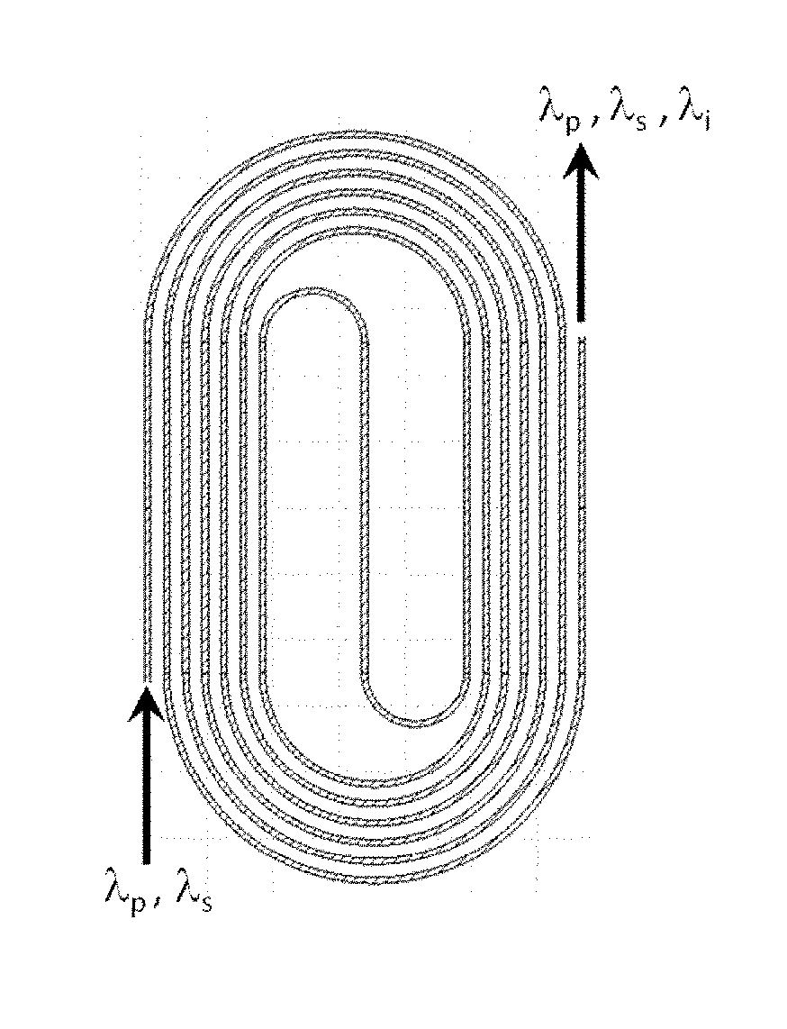
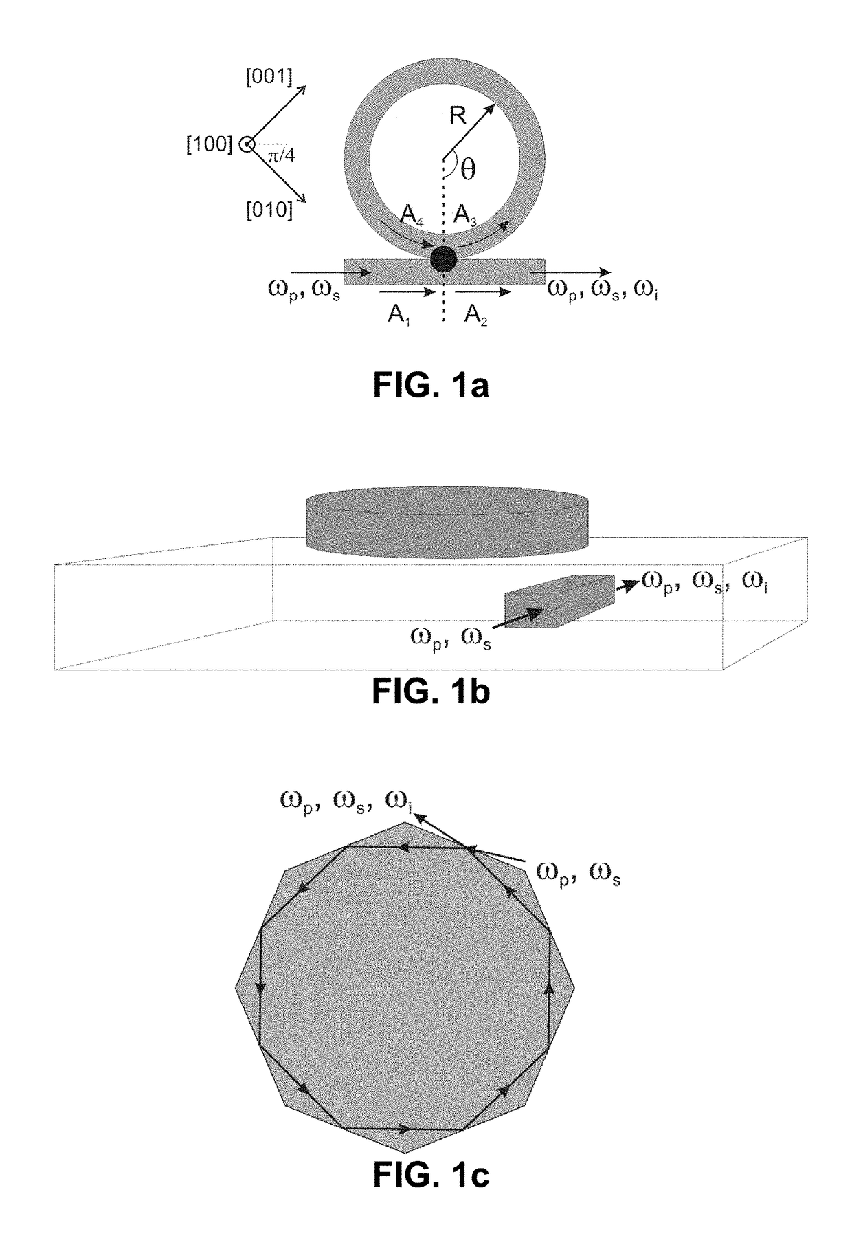
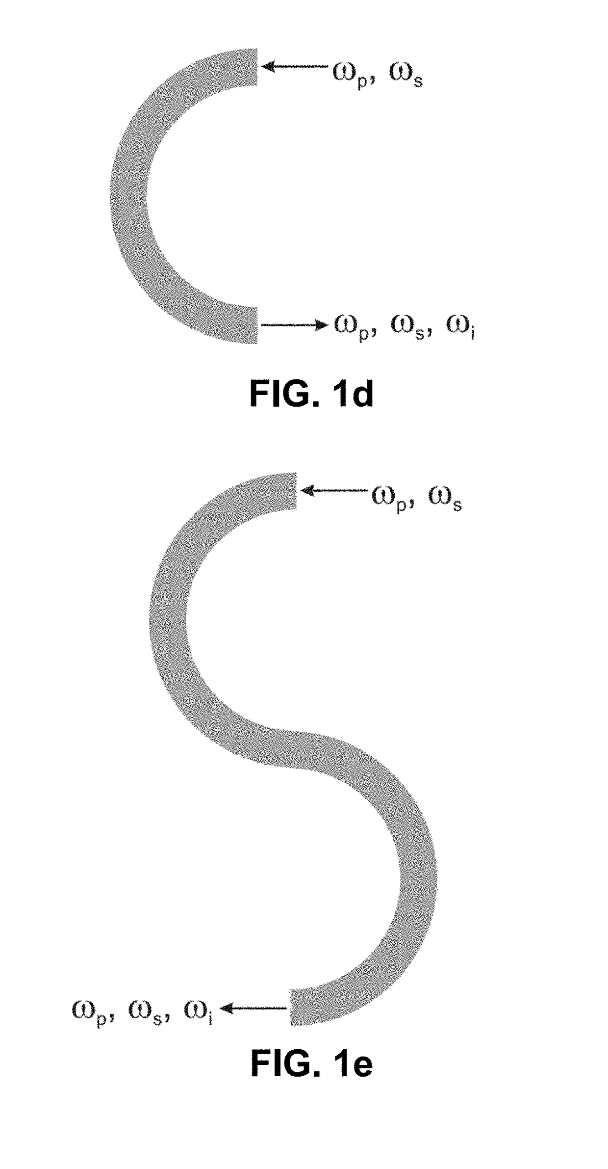
[0161]For the first exemplary comparison in the first embodiment, one considers for the QPM Raman ring converter configuration a TE-polarized pump input and a TE-polarized Stokes-shifted signal input with a frequency difference corresponding to the exact Raman resonance: ωp=1.22×10¹⁵ rad / s (λp=1.55 μm), ωs=1.12×10¹⁵ rad / s (λs=1.686 μm). This leads to a generated idler wave with angular frequency ωi=1.32×10¹⁵ rad / s (λi=1.434 μm). The system may have a structure as illustrated in FIG. 1. At these near-infrared operation wavelengths, the Raman gain coefficient gR of silicon equals 20×10−9 cm / W. As there are no dispersion engineering constraints for the QPM converter, one is free to choose the waveguide geometry for both the ring and the channel. When taking a nanowire of 300-nm height and 500-nm width, the free carrier lifetime τeff will be as short as 500 ps. Because of the oblong core of the nanowire, TM fields generated through spontaneous Raman scattering in the ring are for the la...

second embodiment

[0164]It is pointed out that for the QPM device the TPA losses will also undergo a periodic variation proportional to (0.88+0.12 cos2(2θ)) in the ring, but as the varying part of the TPA losses is small compared to the constant part, this variation only has a small influence, as simulations that are not presented here in detail confirm. In the second embodiment it will be shown, however, that an equally small variation of the effective Kerr nonlinearity γ does suffice to effectively establish quasi-phase-matching in a parametric converter, since this variation establishes a phase effect rather than an intensity loss effect.

[0165]One might question whether the coupling coefficients Kp2=Ks2=Ki2=0.05 assumed here yield the highest conversion efficiencies for the QPM and PPM Raman devices, and whether the ring circumference L=2.1 mm calculated for the QPM converter is the most optimal ring circumference for the PPM converter as well. When varying the coupling coefficients using intermed...

embodiment 3

When sending a current density of 103 A / m through the graphene sheet, deff˜100×10−12 m / V. For the remaining device parameters the following values were taken: waveguide modal area Aeff=0.5 μm2, linear loss α=50 dB / cm, effective two-photon absorption coefficient β=25×10−11 m / W, effective free carrier absorption efficiency φ=6×10⁻¹², effective free carrier lifetime τeff=0.5 ns, Ip,in=2×10¹¹ W / m2, Is,in=2×10⁸ W / m2. , the relatively small effective free carrier absorption efficiency is due to the fact that at the considered pump wavelength only the graphene sheet contributes to free carrier generation, and only a small fraction of these free carriers effectively diffuse to the silicon waveguide. One then can numerically solve equations (13) to (15) for the QPM DFG converter. FIG. 11 shows the distribution along the spiral for the idler intensity. The output idler intensity emerging from the spiral Ii,out equals 4.6×10⁴ W / m2 corresponding to a DFG efficiency Ii,out / Is,in of 36 dB over a ...


PUM

PropertyMeasurementUnit
thicknessaaaaaaaaaa
propagation distancesaaaaaaaaaa
energyaaaaaaaaaa

Abstract

A system for conversion or amplification using quasi-phase matched nonlinear optical wave-mixing includes a first radiation source for providing a pump radiation beam, a second radiation source for providing a signal radiation beam, a bent structure for receiving the pump radiation beam and the signal radiation beam, and an outcoupling radiation propagation portion for coupling out an idler radiation beam generated in the bent structure. A radiation propagation portion of the bent structure is made of a uniform three-dimensional material at least partly covered by a two-dimensional or quasi-two-dimensional material layer and has a dimension taking into account the spatial variation of the nonlinear optical susceptibility along the radiation propagation portion as experienced by radiation traveling along the bent structure for obtaining quasi-phase matched nonlinear optical wave-mixing in the radiation propagation portion. The dimension thereby is substantially inverse proportional with the linear phase mismatch for the nonlinear optical process.

Description

FIELD OF THE INVENTION[0001]The present invention relates to the field of optics. More particularly, the present invention relates to methods and systems for Raman converters, parametric converters and parametric amplifiers with cavity enhancement and with quasi-phase-matching.BACKGROUND OF THE INVENTION[0002]Over the past several decades there has been growing interest in the development of devices based on second-order nonlinear effects such as sum-frequency generation (SFG) and difference frequency generation (DFG) and devices based on third-order nonlinear effects such as Raman-resonant four-wave-mixing (FWM) and Kerr-induced four-wave-mixing (FWM). SFG, DFG and Kerr-induced FWM are parametric light-matter interactions that are not resonant with a material level and that are used in parametric converters and parametric amplifiers. Raman-resonant FWM is a light-matter interaction that is perfectly resonant or almost perfectly resonant with a characteristic energy level of the mat...

Claims


Application Information

Patent Timeline
Patent Type & Authority Patents(United States)
IPC IPC(8): G02F1/35G02F2/02
CPCG02F1/3544G02F1/3501G02F1/3534G02F2001/3548G02F2001/3509G02F1/353G02F1/365G02F1/3509G02F1/3548
Inventor VERMEULEN, NATHALIETHIENPONT, HUGO
Owner VRIJE UNIV BRUSSEL
Learn More