
Electromagnetic wave shielding support base-attached encapsulant, encapsulated substrate having semicondutor devices mounted thereon, encapsulated wafer having semiconductor devices formed thereon, and semiconductor apparatus

a technology of electromagnetic wave shielding and encapsulation, which is applied in the direction of film/foil adhesive, basic electric elements, solid-state devices, etc., can solve the problems of unintended high-frequency energy outside, dead space occurrence, unachievable film thinning, etc., to achieve excellent electromagnetic wave shielding property and reliability, excellent mass-productivity, workability and economical efficiency, excellent

Active Publication Date: 2018-01-09
SHIN ETSU CHEM IND CO LTD
View PDF31 Cites 3 Cited by
  • Summary
  • Abstract
  • Description
  • Claims
  • Application Information

AI Technical Summary

Benefits of technology

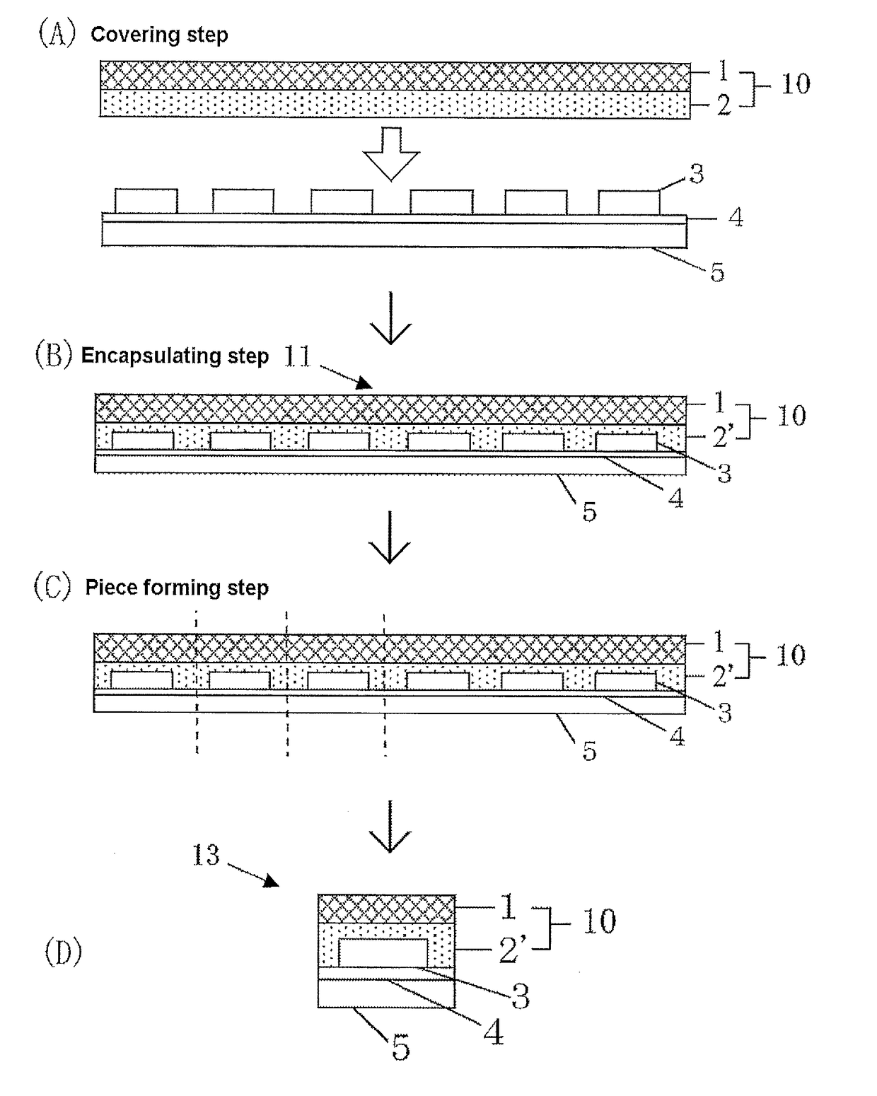
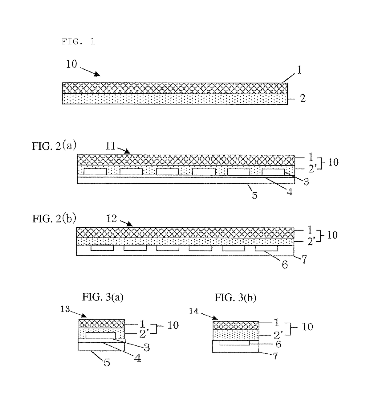
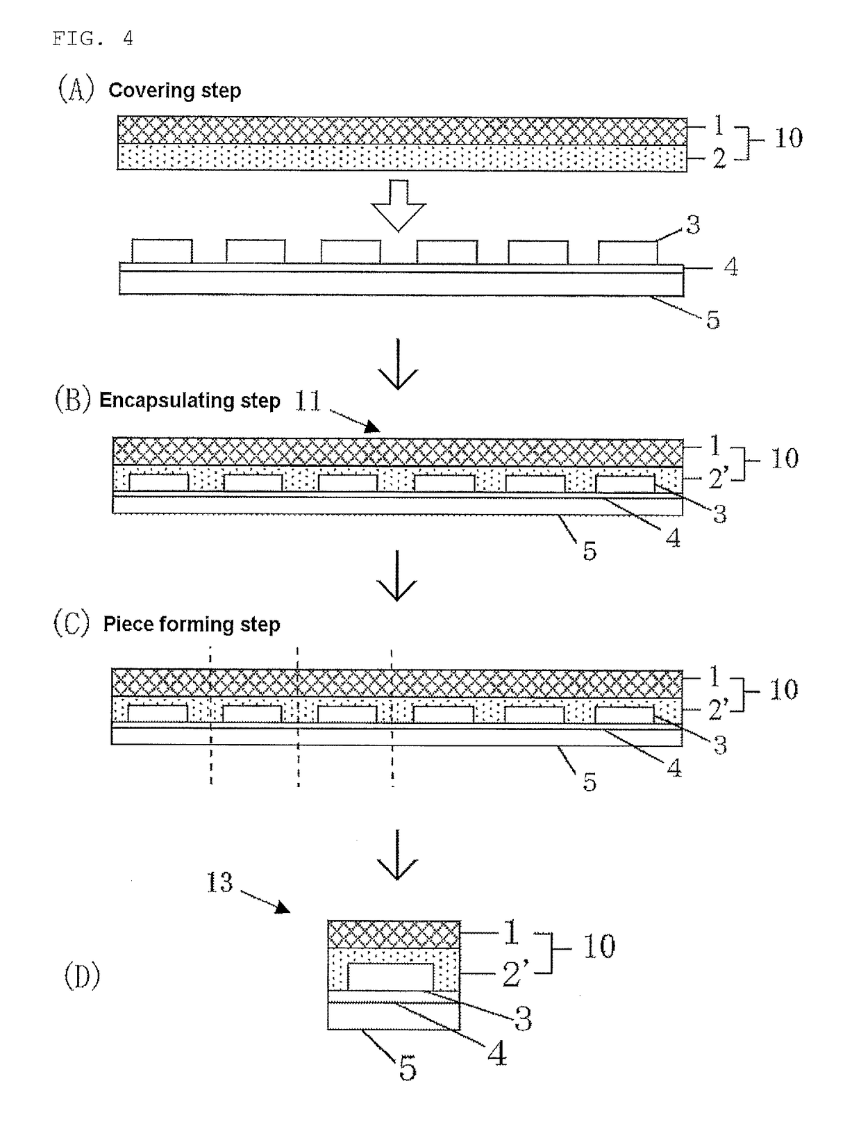
[0015]The present invention has been accomplished in view of the above-mentioned circumstances, and an object thereof is to provide a support base-attached encapsulant that can collectively encapsulate a semiconductor-device mounting surface of a substrate having the semiconductor devices mounted thereon or a semiconductor-device forming surface of a wafer having semiconductor devices formed thereon without occurrence of warping of the substrate or the wafer, peeling of the semiconductor devices from the substrate, and breakage of the wafer even in the case that a large-diameter wafer or a large-area substrate such as inorganic, organic, or metal substrate, especially thin one, is encapsulated, and that has excellent electromagnetic wave shielding property, reliability such as heat resistance and moisture resistance after encapsulating, and extremely high versatility, mass-productivity, workability, and economical efficiency.
[0020]When such an electromagnetic wave shielding support base-attached encapsulant is employed, the support base can suppress the shrinkage stress of the thermosetting resin layer at the time of encapsulating and curing, so that warping of the substrate or the wafer, peeling of the semiconductor devices from the substrate, and breakage of the wafer can be inhibited even in the case that a large-diameter wafer or a large-area substrate such as inorganic, organic, or metal substrate is encapsulated, and the semiconductor device mounting surface of the substrate having the semiconductor devices mounted thereon or the semiconductor device forming surface of the wafer having semiconductor devices formed thereon can be collectively encapsulated. In addition, the inventive support base-attached encapsulant can exhibit excellent electromagnetic wave shielding property and reliability such as heat resistance and moisture resistance after encapsulating. Further, this electromagnetic wave shielding support base-attached encapsulant is extremely excellent in versatility, mass-productivity, workability, and economical efficiency.
[0022]Such a support base enables the electromagnetic wave shielding support base-attached encapsulant to exhibit sufficient electromagnetic wave shielding effect.
[0024]When such a support base is used, the electromagnetic wave shielding support base-attached encapsulant can exhibit more excellent electromagnetic wave shielding property, and can inhibit occurrence of warping of the substrate or the wafer, peeling of the semiconductor devices from the substrate, and breakage of the wafer even in the case that a large-diameter wafer or a large-area substrate such as inorganic, organic, or metal substrate is encapsulated.
[0033]As mentioned above, according to the electromagnetic wave shielding support base-attached encapsulant of the present invention, the support base can suppress the shrinkage stress of the thermosetting resin layer at the time of encapsulating and curing, so that warping of the substrate or the wafer, peeling of the semiconductor devices from the substrate, and breakage of the wafer can be inhibited even in the case that a large-diameter wafer or a large-area substrate such as inorganic, organic, or metal substrate is encapsulated, and the semiconductor device mounting surface of the substrate having the semiconductor devices mounted thereon or the semiconductor device forming surface of the wafer having semiconductor devices formed thereon can be collectively encapsulated. In addition, the inventive support base-attached encapsulant can exhibit excellent electromagnetic wave shielding property and reliability such as heat resistance and moisture resistance after encapsulating. Further, this electromagnetic wave shielding support base-attached encapsulant is extremely excellent in versatility, mass-productivity, workability, and economical efficiency.
[0034]Moreover, in the encapsulated substrate having semiconductor devices mounted thereon and the encapsulated wafer having semiconductor devices formed thereon, which have been encapsulated by the electromagnetic wave shielding support base-attached encapsulant, warping of the substrate or the wafer, peeling of the semiconductor devices from the substrate, and breakage of the wafer are inhibited. Further, the semiconductor apparatus obtained by dicing into each piece the encapsulated substrate having semiconductor devices mounted thereon or the encapsulated wafer having semiconductor devices formed thereon, which has been encapsulated with the electromagnetic wave shielding support base-attached encapsulant excellent in reliability such as heat resistance and moisture resistance and inhibited from warping, is high quality.

Problems solved by technology

In addition, this device emits an unintended high-frequency energy outside.
However, if the sizes of parts within the package are uneven, the sheet metal shield becomes tall because of coating the whole housing with a conductive material or using a metal or metallic mesh cover, which causes problems of occurrence of dead space and unachievable film-thinning due to the accumulation of heat, etc.
When a large-area substrate or a large-diameter wafer of 300 mm (12 inches) or more is encapsulated, there is a problem that the substrate or the wafer occasionally warps due to shrinkage stress of the epoxy resin or the like at the time of encapsulating and curing, and especially, the large-diameter wafer with thin thickness is liable to warp.
In addition, when a semiconductor-device mounting surface of a large-area substrate having semiconductor devices mounted thereon is encapsulated, a problem arises that the semiconductor devices are peeled from the substrate by shrinkage stress of the epoxy resin or the like at the time of encapsulating and curing.
Accordingly, there is a big problem that encapsulated large-area substrates and large-diameter wafers cannot be used for mass-production.

Method used


Image

  • Electromagnetic wave shielding support base-attached encapsulant, encapsulated substrate having semicondutor devices mounted thereon, encapsulated wafer having semiconductor devices formed thereon, and semiconductor apparatus
  • Electromagnetic wave shielding support base-attached encapsulant, encapsulated substrate having semicondutor devices mounted thereon, encapsulated wafer having semiconductor devices formed thereon, and semiconductor apparatus
  • Electromagnetic wave shielding support base-attached encapsulant, encapsulated substrate having semicondutor devices mounted thereon, encapsulated wafer having semiconductor devices formed thereon, and semiconductor apparatus

Examples


synthesis example 1

Organosilicon Compound Having Nonconjugated Double Bond (A1)

[0203]27 mol of organosilane represented by PhSiCl3, 1 mol of ClMe2SiO(Me2SiO)33SiMe2Cl, and 3 mol of MeViSiCl2 were dissolved in a toluene solvent. The solvent was then added dropwise into water, co-hydrolyzed, washed with water, neutralized by alkali washing, dehydrated, and stripped to synthesize an organosilicon compound having a nonconjugated double bond (A1).

[0204]The composition ratio of constituent units in this compound is represented by the formula: [PhSiO3 / 2]0.27 [—SiMe2O—(Me2SiO)33—SiMe2O—]0.01[MeViSiO2 / 2]0.03. The weight average molecular weight of the compound was 62,000, and the melting point was 60° C. It is to be noted that Vi in the composition formula denotes a vinyl group represented by (—C═C).

synthesis example 2

Organohydrogenpolysiloxane (B1)

[0205]27 mol of organosilane represented by PhSiCl3, 1 mol of ClMe2SiO(Me2SiO)33SiMe2Cl, and 3 mol of MeHSiCl2 were dissolved in a toluene solvent. The solvent was then added dropwise into water, co-hydrolyzed, washed with water, neutralized by alkali washing, dehydrated, and stripped to synthesize organohydrogenpolysiloxane (B1).

[0206]The composition ratio of constituent units of this resin is represented by the formula: [PhSiO3 / 2]0.27[—SiMe2O-(Me2SiO)33—SiMe2O-]0.01[MeHSi2 / 2]0.03. The weight average molecular weight of the resin was 58,000, and the melting point was 58° C.

preparation example 1

[0207]A 300-mesh stainless steel wire net (mesh: 300 mesh / 2.54 cm, opening size: 55 μm, open area ratio: 42%, wire diameter: 30 μm, thickness: 70 μm) was impregnated with 3-aminopropyltrimethoxysilane (Product name: KBM-903, available from Shin-Etsu Chemical Co., Ltd.) used as the organosilicon compound, and the impregnated material was dried under heating at 100° C. for 10 minutes. Thereafter, the resultant material was subjected to heat treatments at 100° C. for 1 hour and 200° C. for 1 hour to prepare an electromagnetic wave shielding support base (1-a).

[0208]As regards electromagnetic wave shielding property of this support base, the following results were obtained.[0209]Measuring method: KEC method[0210]Measurement results: 100 MHz 60 dB[0211]300 MHz 48 dB[0212]500 MHz 45 dB[0213]1,000 MHz 32 dB

[0214]Thus, electromagnetic wave shielding property was found.


PUM

PropertyMeasurementUnit
electromagnetic wave shielding propertyaaaaaaaaaa
diameteraaaaaaaaaa
electromagnetic wave shielding propertyaaaaaaaaaa

Abstract

The present invention provides an electromagnetic wave shielding support base-attached encapsulant for collectively encapsulating a semiconductor device mounting surface of a substrate having semiconductor devices mounted thereon or a semiconductor device forming surface of a wafer having semiconductor devices formed thereon, the support base-attached encapsulant including a support base having an electromagnetic wave shielding property of 20 dB or more within a range of 100 MHz to 1,000 MHz, and an encapsulant composed of a thermosetting resin layer laminated on the support base. There can be provided a support base-attached encapsulant that can collectively encapsulate a semiconductor device mounting surface of a substrate having the semiconductor devices mounted thereon or a semiconductor device forming surface of a wafer having semiconductor devices formed thereon without occurrence of warping of the substrate or the wafer, peeling of the semiconductor devices from the substrate, and breakage of the wafer even in the case that a large-diameter wafer or a large-area substrate such as inorganic, organic, or metal substrate, especially thin one, is encapsulated, and that has excellent electromagnetic wave shielding property, reliability such as heat resistance and moisture resistance after encapsulating, and extremely high versatility, mass-productivity, workability, and economical efficiency.

Description

BACKGROUND OF THE INVENTION[0001]Field of the Invention[0002]The present invention relates to an electromagnetic wave shielding support base-attached encapsulant, an encapsulated substrate having semiconductor devices mounted thereon and an encapsulated wafer having semiconductor devices formed thereon each using the encapsulant, and a semiconductor apparatus manufactured from these.[0003]Description of the Related Art[0004]With remarkable progress of digital technology, miniaturization and higher performance of electronic devices represented by personal computers and mobile phones have been required. For example, a printed wiring substrate, which is a representative part of these devices, has been improved toward high density mounting and miniaturization. Along with this current, an electronic device having highly integrated semiconductor parts is formed with a circuit that tends to sensitively respond to outside noise and cause malfunctions or failures. In addition, this device em...

Claims


Application Information

Patent Timeline
Patent Type & Authority Patents(United States)
IPC IPC(8): H01L23/06H01L23/552H01L23/31H01L23/29H01L21/56H01L23/00C09J7/22
CPCC09J7/28C09J7/29H01L23/06H01L21/561H01L23/29H01L23/295H01L23/3121H01L23/552H01L24/94H01L24/97H01L2924/3511H01L2924/3025H01L2924/181H01L2924/10253H01L2924/0002H01L2224/97H01L2224/16227C09J2201/61C09J2201/622C09J2203/326C09J2400/163H01L24/13H01L24/16H01L2224/13111H01L2924/00H01L2924/00012H01L2224/81H01L2924/01047H01L21/78C09J7/22C09J2301/304C09J2301/312
Inventor AKIBA, HIDEKINAKAMURA, TOMOAKISHIOBARA, TOSHIOYAMAGUCHI, SHINSUKE
Owner SHIN ETSU CHEM IND CO LTD
Learn More