Ultra high density thin film transistor substrate having low line resistance structure and method for manufacturing the same

a technology of ultra-high density thin film transistors and line resistance structures, which is applied in the direction of instruments, semiconductor devices, electrical equipment, etc., can solve the problems of reducing the aperture ratio of the display area, the video quality of the display device, and the difficulty in selecting a material with a lower resistivity, etc., and achieves low resistance bus line structure, high density, and high density

Active Publication Date: 2017-12-05
LG DISPLAY CO LTD
View PDF12 Cites 0 Cited by
  • Summary
  • Abstract
  • Description
  • Claims
  • Application Information

AI Technical Summary

Benefits of technology

[0022]In order to overcome the above mentioned drawbacks, the purpose of the present disclosure is to suggest an ultra high density thin film transistor substrate having a low resistance bus line structure for large area and ultra high density flat panel display device and a method for manufacturing the same. Another purpose of the present disclosure is to suggest an ultra high density thin film transistor substrate having a low resistance bus line structure in which the line resistance is not increased even though the width of the line is being narrowed because that the thickness of the bus line is being thicker and a method for manufacturing the same. Still another purpose of the present disclosure is to suggest an ultra high density thin film transistor substrate having a low resistance bus line structure in which the bus line has the double layered structure as having good uniformity of the bus line layers and double the thickness. Yet another purpose of the present disclosure is to suggest an ultra high density thin film transistor substrate having a low resistance bus line structure and a method for manufacturing the same without increasing the complexity of the manufacturing steps and the tack time for the manufacturing, just by adding additional bus lines stacked on the bus line.

Problems solved by technology

The LCD according to the related art explained above has a problem to have a large display area.
As a result, the display device has the video quality problems.
To select a material having a lower resistivity is very difficult because the material is limited.
In that case, the aperture ratio of the display area is also reduced and it causes another reason of defected display quality.
For another example, by enlarging the thickness of the bus lines, the etching tact time should be longer and longer when forming the bus lines and the space between the bus lines should be increased, so that it can cause the problem of lowered aperture ratio.
Furthermore, as increasing the thickness of the bus line, the step difference between the bus line and other layer can be enlarged so that it causes the defects at rubbing process of the alignment layer.

Method used


Image

  • Ultra high density thin film transistor substrate having low line resistance structure and method for manufacturing the same
  • Ultra high density thin film transistor substrate having low line resistance structure and method for manufacturing the same
  • Ultra high density thin film transistor substrate having low line resistance structure and method for manufacturing the same

Examples


Embodiment Construction

[0030]Referring to attached figures, we will explain preferred embodiments of the present disclosure. Like reference numerals designate like elements throughout the detailed description. However, the present disclosure is not restricted by these embodiments but can be applied to various changes or modifications without changing the technical spirit. In the following embodiments, the names of the elements are selected by considering the easiness for explanation so that they may be different from actual names.

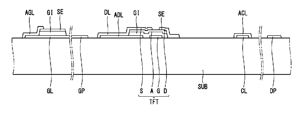
[0031]Hereinafter, referring to attached figures including FIG. 3 and FIGS. 4A to 4E, we will explain preferred embodiments of the present disclosure. FIG. 3 is a plane view illustrating the structure of the ultra high density thin film transistor substrate used in the large area horizontal electric field type liquid crystal display according to the present disclosure. FIGS. 4A to 4E are cross-sectional views illustrating the steps of manufacturing for the ultra high density thin...


PUM

PropertyMeasurementUnit
widthaaaaaaaaaa
widthaaaaaaaaaa
widthaaaaaaaaaa

Abstract

A display device is described that has reduced resistance in one or more of the gate, common, data electrical lines that control the operation of the pixels of the display device. Reduced resistance is achieved by forming additional metal and / or metal-alloy layers on the gate, common, and / or data lines in such a manner so that the cross-sectional area of those lines is increased. As a consequence, each such line is formed so as to be thicker than could otherwise be achieving without causing defects in the rubbing process of an alignment layer. Additionally, no widening of these lines is needed, thus preserving the aspect ratio of the device. The gate insulating and semiconducting layers that in part make up the thin film transistors that help control the operation of the pixels of the device may also be designed to take into account the increased thickness of the lines.

Description

[0001]This application claims the benefit of Korea Patent Application No. 10-2015-0100406 filed on Jul. 15, 2015, which is incorporated herein by reference for all purposes as if fully set forth herein.BACKGROUND OF THE INVENTION[0002]Field of the Invention[0003]The present disclosure relates to an ultra high density thin film transistor (or “TFT”) substrate having low resistance bus line structure and a method for manufacturing the same. Especially, the present disclosure relates to an ultra high density TFT substrate having double-thick bus lines by forming the double layered gate line and data line to have low resistance bus line structure and a method for manufacturing the same.[0004]Discussion of the Related Art[0005]Nowadays, various flat panel display devices are developed for overcoming many drawbacks of the cathode ray tube such as heavy weight and bulk volume. The flat panel display devices include the liquid crystal display device (or LCD), the field emission display (or ...

Claims


Application Information

Patent Timeline
Patent Type & Authority Patents(United States)
IPC IPC(8): H01L27/12G02F1/1362G02F1/1343
CPCH01L27/124G02F1/136286H01L27/1237H01L27/1262H01L27/1288G02F2201/40G02F1/134363G02F2001/13629G02F2001/136295G02F1/1368H01L27/1259G02F1/13629G02F1/136295
Inventor JEONG, YOUNGMINSHIN, SEUNGHWANSEO, DAEYOUNGLEE, SOYOUNG
Owner LG DISPLAY CO LTD
Why Eureka
Try Eureka