Communication device, router having communication device, bus system, and circuit board of semiconductor circuit having bus system

a communication device and bus system technology, applied in the field of communication devices, methods and programs in the semiconductor system having a bus, can solve the problem of more difficult design of integrated circuits based on a centralized bus control, and achieve the effect of reinforcing the error tolerance function of an existing noc and reducing the area and process overhead

Active Publication Date: 2017-10-24
PANASONIC INTELLECTUAL PROPERTY MANAGEMENT CO LTD
View PDF13 Cites 0 Cited by
  • Summary
  • Abstract
  • Description
  • Claims
  • Application Information

AI Technical Summary

Benefits of technology

[0011]The prior art technique needs further improvement to maintain the bus transmission performance of an NoC. For example, it is required to perform error corrections at necessary locations and at necessary timings, and to prevent transmissions with transmission errors uncorrected. There is also a demand for reducing the area and the process overhead, and for reinforcing the error tolerance function of an existing NoC in a simple manner.
[0012]A non-limiting example embodiment of the present application provides a technique for reducing the footprint and the process overhead and for reinforcing the error tolerance function in a simple manner.
[0015]An example embodiment of the present disclosure provides a network connection in a network on chip or a network connection between System On Chips (SoCs), whereby it is possible to reduce the footprint and the process overhead and to reinforce the error tolerance function in a simple manner.

Problems solved by technology

However, an integrated circuit now has an enhanced functionality and multiple cores, thereby increasing the circuit scale, with traffic flows flowing through the bus while varying in a complicated manner, thus making it more difficult to design an integrated circuit based on a centralized bus control.

Method used


Image

  • Communication device, router having communication device, bus system, and circuit board of semiconductor circuit having bus system
  • Communication device, router having communication device, bus system, and circuit board of semiconductor circuit having bus system
  • Communication device, router having communication device, bus system, and circuit board of semiconductor circuit having bus system

Examples


first embodiment

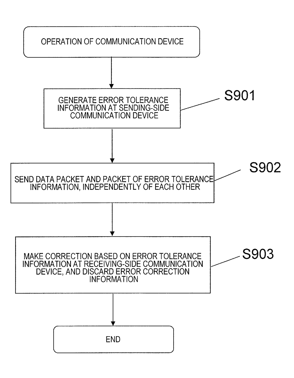
[0048]the present disclosure is a communication device for use in a bus system of a semiconductor circuit having a sending node and a receiving node and including a bus over which data is transmitted by a packet switching scheme. The communication device includes: a receiving terminal which receives one or more packets via a bus; a storage device which stores a rule in which a condition regarding a bus system operation environment and an error tolerance scheme are associated with each other, and information regarding a path length; an error processor which determines the error tolerance scheme by utilizing the condition regarding the bus system operation environment and the rule so as to generate error tolerance information corresponding to the received data according to the determined error tolerance scheme; and a sending terminal which sends at least one packet including the error tolerance information and the data to the bus. The condition regarding the bus system operation envir...

second embodiment

[0057]the present disclosure is a communication device for use in a bus system of a semiconductor circuit having a sending node and a receiving node for transmitting data by a packet switching scheme. The communication device includes: a receiving terminal which receives at least one packet including data and error tolerance information; an error processor which carries out an error correction process for a packet of the data by utilizing the error tolerance information; and a sending terminal which sends the packet of data having undergone the error correction process to the receiving node.

[0058]One embodiment of the present disclosure is a router for use in the bus system for relaying the packet, the router including the communication device set forth above.

[0059]One embodiment of the present disclosure is a bus system of a semiconductor circuit including: a sending node which sends one or more packets including data; a first communication device of claim 1 receiving the one or mo...


PUM


Abstract

A communication device includes: a receiving terminal; a storage device which stores a rule in which a condition regarding a bus system operation environment and an error tolerance scheme are associated with each other, and information regarding a path length; an error processor which determines the error tolerance scheme by utilizing the condition regarding the bus system operation environment and the rule so as to generate error tolerance information corresponding to the received data according to the determined error tolerance scheme; and a sending terminal for sending at least one packet including the error tolerance information and the data to the bus. The operation environment-related condition is a condition for granting an error tolerance for a transmission path of which a bus path length to another communication device, which is a destination of the data, is greater than a predetermined value.

Description

[0001]This is a continuation of International Application No. PCT / JP2013 / 006547, with an international filing date of Nov. 6, 2013, which claims priority of Japanese Patent Application No. 2012-261013, filed on Nov. 29, 2012, the contents of which are hereby incorporated by reference.BACKGROUND[0002]1. Technical Field[0003]The present disclosure relates to a communication device, method and program in a semiconductor system having a bus.[0004]2. Description of the Related Art[0005]FIG. 1(a) shows an example centralized bus control. With a conventional integrated circuit performing a centralized bus control, the connection between a plurality of bus masters and a memory device is primarily made by a single bus, and an arbiter arbitrates between bus masters for access to the memory device. However, an integrated circuit now has an enhanced functionality and multiple cores, thereby increasing the circuit scale, with traffic flows flowing through the bus while varying in a complicated m...

Claims


Application Information

Patent Timeline
Patent Type & Authority Patents(United States)
IPC IPC(8): G06F11/00G06F11/07H04L1/00
CPCG06F11/076G06F11/0745H04L1/0086H04L1/0041H04L2001/0094
Inventor YAMAGUCHI, TAKAOYOSHIDA, ATSUSHIISHII, TOMOKITOKUTSU, SATORU
Owner PANASONIC INTELLECTUAL PROPERTY MANAGEMENT CO LTD
Why Eureka
Try Eureka