Multilayer ceramic capacitor, multilayer ceramic capacitor series including the same, and multilayer ceramic capacitor mount body including the same
a multi-layer ceramic capacitor and ceramic capacitor technology, applied in the direction of fixed capacitors, stacked capacitors, fixed capacitor details, etc., can solve the problems of cracks and cracks (delamination), and achieve the effect of reducing or preventing cracks and sufficient electrostatic capacitan
- Summary
- Abstract
- Description
- Claims
- Application Information
AI Technical Summary
Benefits of technology
Problems solved by technology
Method used
Image
Examples
first preferred embodiment
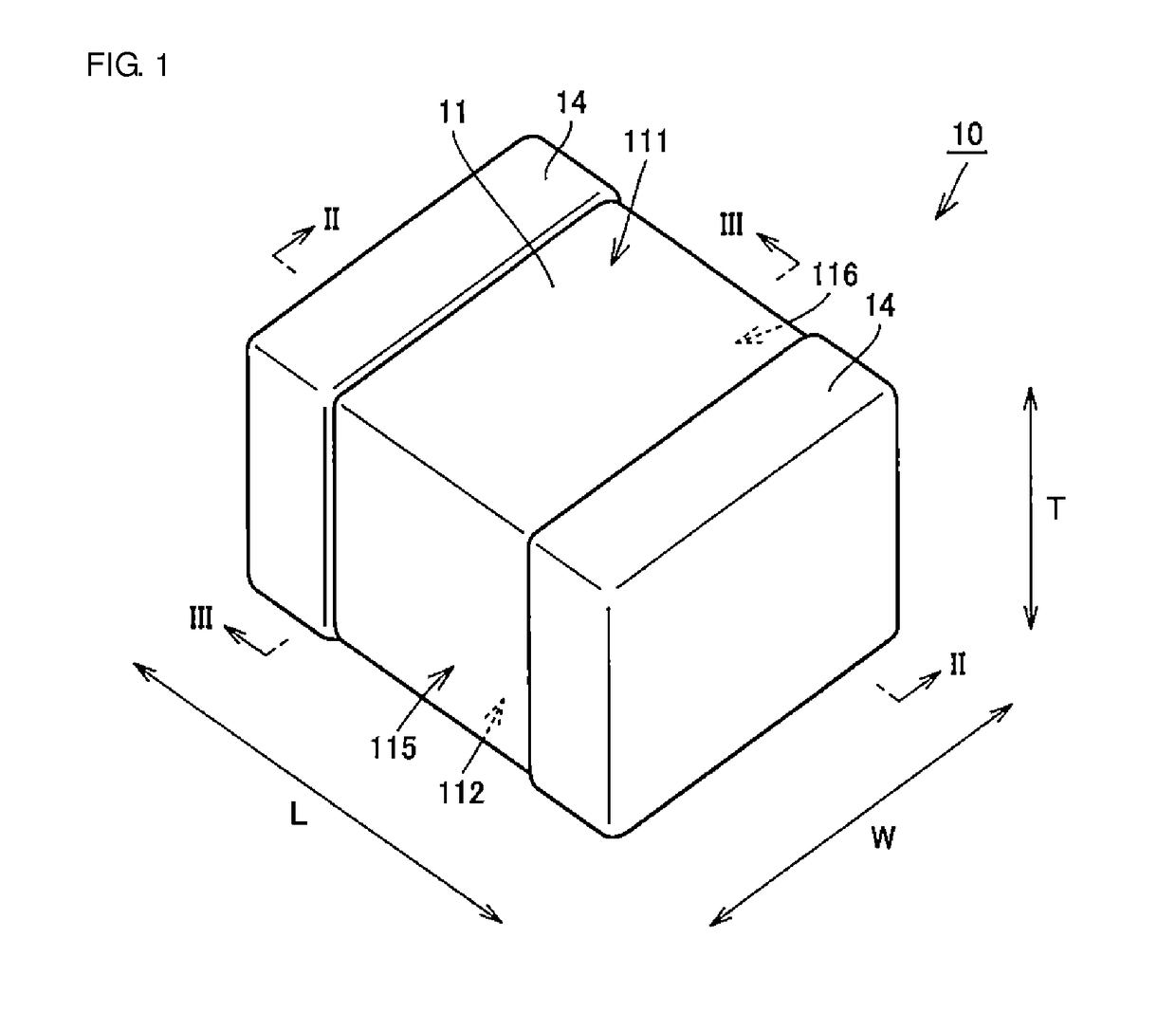
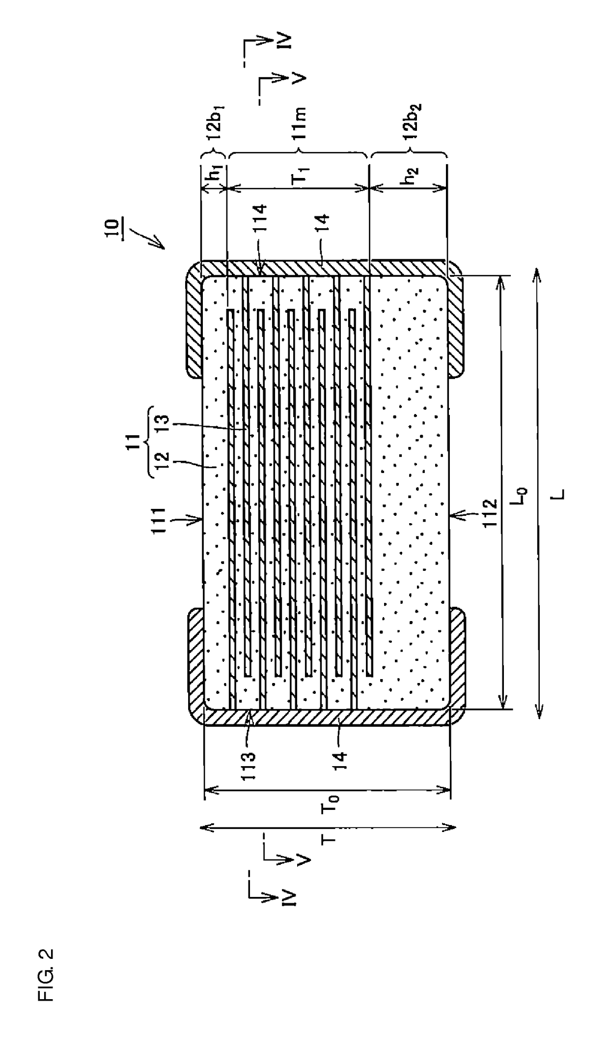
[0045]FIG. 1 is an external perspective view of a capacitor according to a first preferred embodiment of the present invention. FIGS. 2 and 3 are sectional views taken along lines II-II and III-III, respectively, of FIG. 1. FIGS. 4 and 5 are sectional views taken along lines IV-IV and V-V, respectively, of FIG. 2. In FIGS. 1 through 5, the length direction of a body 11, which will be discussed below, is indicated by L, the width direction thereof is indicated by W, and the height direction thereof is indicated by T.
[0046]As shown in FIGS. 1 through 5, the capacitor 10 includes the body 11 and two outer electrodes 14. The body 11 includes a plurality of dielectric layers 12 and a plurality of conductive layers 13 stacked on each other, and has first and second main surfaces 111 and 112 opposing each other in the stacking direction. The two outer electrodes 14 are disposed on some surfaces of the body 11 and are electrically connected to some of the plurality of conductive layers 13.
[...
second preferred embodiment
[0104]FIG. 10 is an external perspective view of a capacitor 10a according to the second preferred embodiment of the present invention. FIGS. 11 and 12 are sectional views taken along lines XI-XI and XII-XII, respectively, of FIG. 10. FIGS. 13 and 14 are sectional views taken along lines XIII-XIII and XIV-XIV, respectively, of FIG. 11. In FIGS. 10 through 14, the length direction of a body 11 is indicated by L, the width direction thereof is indicated by W, and the height direction thereof is indicated by T.
[0105]As shown in FIGS. 10 through 14, the capacitor 10a includes the body 11 and two outer electrodes 14. The body 11 includes a plurality of dielectric layers 12 and a plurality of conductive layers 13 stacked on each other, and includes first and second main surfaces 111 and 112 opposing each other in the stacking direction. The two outer electrodes 14 are disposed on some surfaces of the body 11 and are electrically connected to all the conductive layers 13.
[0106]The pluralit...
third preferred embodiment
[0179]The configuration of the boundary region of the outer portion 12b22 with the inner portion 12b21 of the body 11 of the capacitor is preferably implemented by a pressure-bonding method for a set of mother sheets. Accordingly, the pressure-bonding method for a set of mother sheets in the third preferred embodiment will first be described below.
[0180]FIG. 20 is a sectional view illustrating a state in which a set of mother sheets defining the capacitor in the third preferred embodiment are being pressure-bonded. The set of mother sheets shown in FIG. 20 is that as viewed from the same cross section as that shown in FIG. 17. In FIG. 20, the set of mother sheets corresponding to only two partial bodies 11p is shown.
[0181]As shown in FIG. 20, in the third preferred embodiment, a plurality of mother sheets defining the first outer layer portion 12b1, a plurality of mother sheets defining the inner layer portion 11m, and a plurality of mother sheets defining the inner portion 12b21 ar...
PUM
| Property | Measurement | Unit |
|---|---|---|
| height | aaaaa | aaaaa |
| height | aaaaa | aaaaa |
| height | aaaaa | aaaaa |
Abstract
Description
Claims
Application Information
 - R&D
- Intellectual Property
- Life Sciences
- Materials
- Tech Scout
- Unparalleled Data Quality
- Higher Quality Content
- 60% Fewer Hallucinations
Browse by: Latest US Patents, China's latest patents, Technical Efficacy Thesaurus, Application Domain, Technology Topic, Popular Technical Reports.
© 2025 PatSnap. All rights reserved.Legal|Privacy policy|Modern Slavery Act Transparency Statement|Sitemap|About US| Contact US: help@patsnap.com


