
Junction formation with reduced CEFF for 22NM FDSOI devices

a junction formation and junction technology, applied in the field of semiconductor device formation of silicononinsulator (soi) semiconductor devices, can solve the problems of limited gate dielectric scaling, substantially affecting the performance of mos transistors, and the conductivity of the channel region

Active Publication Date: 2017-04-25
GLOBALFOUNDRIES US INC
View PDF1 Cites 8 Cited by
  • Summary
  • Abstract
  • Description
  • Claims
  • Application Information

AI Technical Summary

Benefits of technology

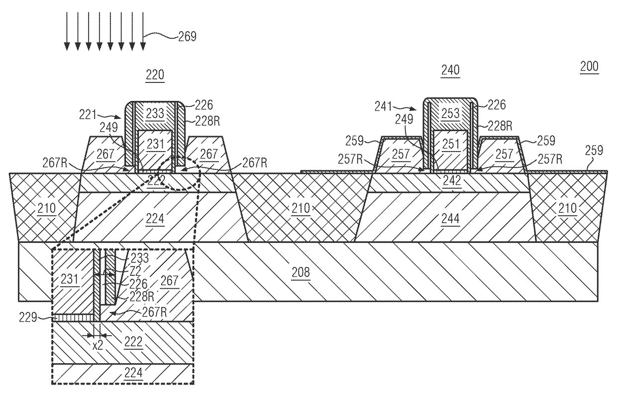
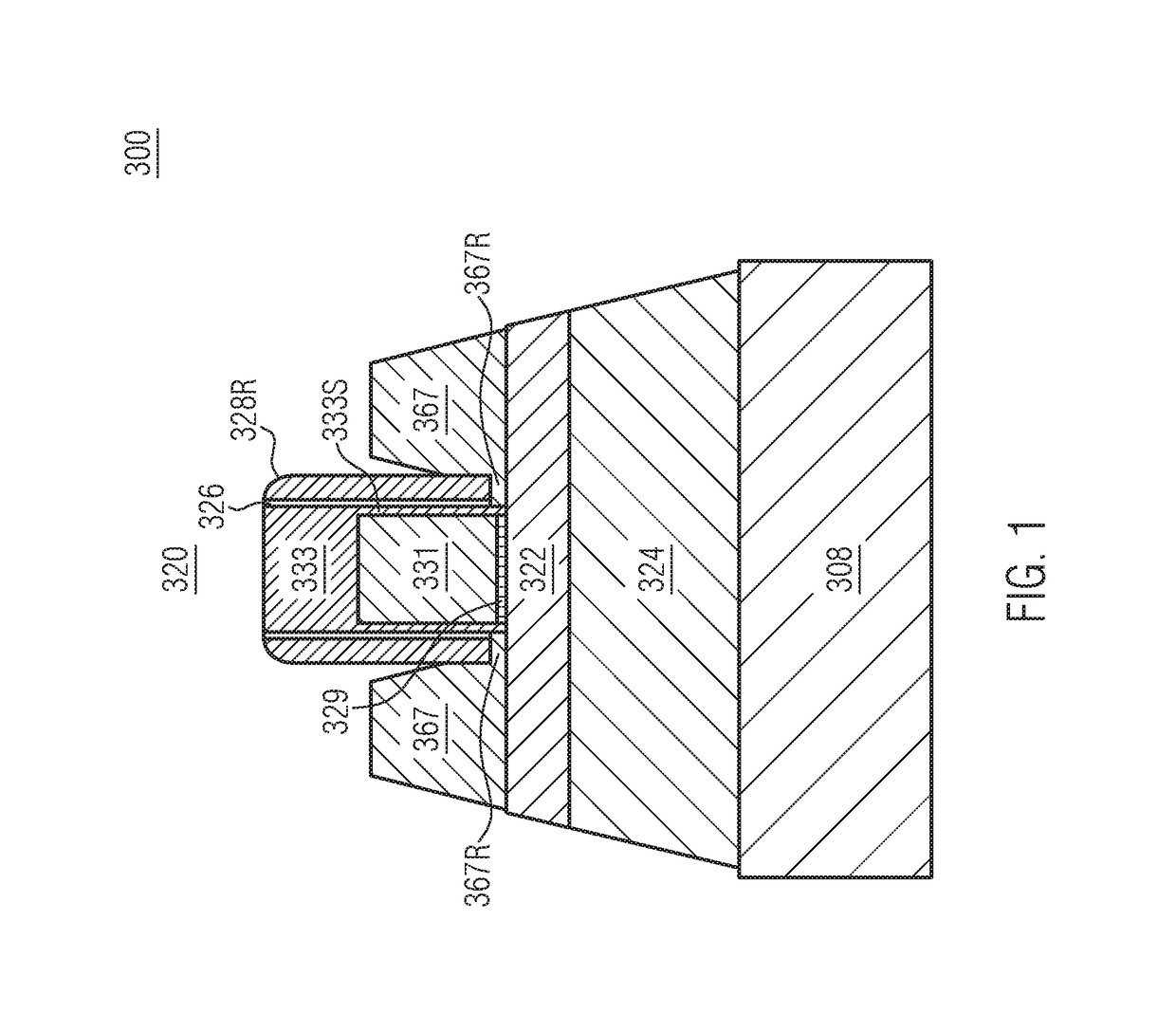
The patent text describes a method and structure for improving the performance of transistors in semiconductor devices. The method involves using a silicon-on-insulator (SOI) substrate with a shallow trench isolation region to electrically isolate transistor devices from each other. The transistor device includes a gate structure with a cap layer, an oxide liner, and a recess on the semiconductor layer where raised source / drain regions are formed. The method results in enhanced transistor performance for both N-channel and P-channel transistors. The patent also describes a semiconductor device that includes the improved transistor structure.

Problems solved by technology

Hence, in combination with the capability of rapidly creating a conductive channel below the insulating layer upon application of the control voltage to the gate electrode, the conductivity of the channel region substantially affects the performance of MOS transistors.
The scaling of the gate dielectric is limited by several factors, such as defects, power supply voltage, time-dependent dielectric breakdown and leakage currents.

Method used


Image

  • Junction formation with reduced C<sub>EFF </sub>for 22NM FDSOI devices
  • Junction formation with reduced C<sub>EFF </sub>for 22NM FDSOI devices
  • Junction formation with reduced C<sub>EFF </sub>for 22NM FDSOI devices

Examples


Embodiment Construction

[0018]Various illustrative embodiments of the invention are described below. In the interest of clarity, not all features of an actual implementation are described in this specification. It will of course be appreciated that in the development of any such actual embodiment, numerous implementation-specific decisions must be made to achieve the developers' specific goals, such as compliance with system-related and business-related constraints, which will vary from one implementation to another. Moreover, it will be appreciated that such a development effort might be complex and time-consuming, but would nevertheless be a routine undertaking for those of ordinary skill in the art having the benefit of this disclosure.

[0019]The following embodiments are described in sufficient detail to enable those skilled in the art to make use of the disclosure. It is to be understood that other embodiments would be evident, based on the present disclosure, and that system, structure, process or mec...


PUM


Abstract

A method of forming a semiconductor device is disclosed including providing a silicon-on-insulator substrate comprising a semiconductor bulk substrate, a buried oxide layer formed on the semiconductor bulk substrate and a semiconductor layer formed on the buried oxide layer, and forming a transistor device on the silicon-on-insulator substrate including providing a gate structure on the semiconductor layer having a gate electrode and a first cap layer on the gate electrode, growing an oxide liner on the transistor device having a first part covering the gate structure and a second part covering the semiconductor layer, forming a second cap layer on the oxide liner, at least partially removing the second part of the oxide liner underneath the second cap layer and the first part of the oxide liner, and epitaxially forming raised source / drain regions on the semiconductor layer.

Description

BACKGROUND[0001]1. Field of the Disclosure[0002]Generally, the present disclosure relates to the fabrication of integrated circuits and semiconductor devices, and, more particularly, to forming silicon-on-insulator (SOI) semiconductor devices.[0003]2. Description of the Related Art[0004]The fabrication of advanced integrated circuits, such as CPUs, storage devices, application specific integrated circuits (ASICs) and the like, requires the formation of a large number of circuit elements on a given chip area according to a specified circuit layout. In a wide variety of electronic circuits, field effect transistors represent one important type of circuit element that substantially determines performance of the integrated circuits. Generally, a plurality of process technologies are currently practiced for forming field effect transistors (FETs), wherein, for many types of complex circuitry, metal-oxide-semiconductor (MOS) technology is currently one of the most promising approaches due...

Claims


Application Information

Patent Timeline
IPC IPC(8): H01L21/336H01L21/311H01L21/02H01L29/06H01L29/78H01L29/66H01L29/08H01L29/417H01L29/165
CPCH01L29/0642H01L29/0847H01L29/41783H01L29/165H01L29/7848H01L29/66636H01L21/0217H01L21/31111H01L29/78H01L21/84H01L29/6653H01L29/6656H01L29/66628H01L29/66772H01L29/78684H01L27/0922H01L27/1203H01L29/16
Inventor THEES, HANS-JUERGENBAARS, PETER
Owner GLOBALFOUNDRIES US INC
Learn More