Semiconductor device and method for manufacturing the same

a semiconductor device and semiconductor technology, applied in the field of semiconductor devices, can solve the problems of many problems such as the inability of nmos and pmos transistors to properly perform their functions, the size of semiconductor devices is reduced, and the distance between the source and drain junction is reduced, so as to achieve the effect of reducing the design rule of the semiconductor device, and reducing the distance between the source and drain junction

Inactive Publication Date: 2005-03-24
SAMSUNG ELECTRONICS CO LTD
View PDF10 Cites 9 Cited by
  • Summary
  • Abstract
  • Description
  • Claims
  • Application Information

AI Technical Summary

Benefits of technology

[0020] As described above, in a semiconductor device and a method for manufacturing the semiconductor device, a junction blocking insulating film is formed on a channel connecting source and drain junctions disposed under a gate stack of a MOS transistor. Thus, since the junction blocking insulating film isolates the source and drains junctions, a design rule of the semiconductor device is reduced. As a result, although a distance between the source and drain junctions is reduced, a short circuit caused by the unwanted diffusion of junctions occurring when the semiconductor device operates can be efficiently prevented.

Problems solved by technology

As the density of semiconductor devices has significantly increased, the design rule has also been reduced, resulting in a decrease in size of semiconductor devices.
As a result, many problems occur when devices such as transistors are formed.
However, with the scaling of semiconductor devices, the NMOS and PMOS transistors cannot properly perform their functions due to a short circuit between junctions in a bulk region.
However, even with the shallow source / drain junctions, because semiconductor devices need to be more scaled, the design rule is likewise reduced.
Accordingly, in the prior art, because the distances between source and drain regions become too short, source and drain junctions can come in contact with each other, causing a short circuit between source / drain junctions in a bulk region.

Method used


Image

  • Semiconductor device and method for manufacturing the same
  • Semiconductor device and method for manufacturing the same
  • Semiconductor device and method for manufacturing the same

Examples


Embodiment Construction

[0025] Hereinafter, preferred embodiments of the present invention will be described in detail with reference to the attached drawings. However, the preferred embodiments of the present invention may be modified into many different ways. The scope of the present invention is, therefore, not limited to the particular embodiments. Rather, the preferred embodiments herein are provided by way of example only.

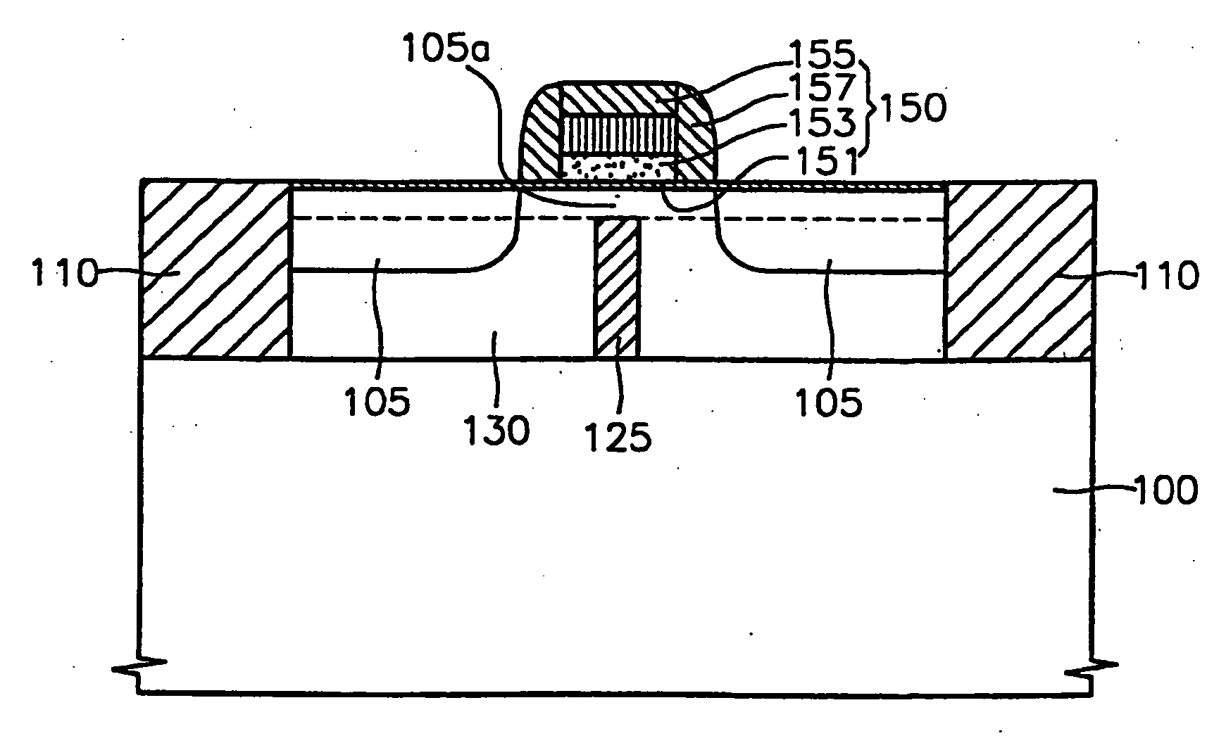
[0026]FIG. 1 is a cross-sectional view of a semiconductor device according to an embodiment of the present invention. Referring to FIG. 1, the semiconductor device according to the present invention includes an isolation insulating film 110, an epitaxial layer 130, a junction blocking insulating film 125, a gate stack 150, and source and drain junctions 105. The isolation insulating film 110 is formed on a semiconductor substrate 100 to a predetermined thickness and defines an active area in which devices will be formed. The epitaxial layer 130 is stacked on the semiconductor subst...


PUM


Abstract

Provided are a semiconductor device and a method for manufacturing the semiconductor device. The semiconductor device includes an isolation insulating film, an epitaxial silicon layer, a junction blocking insulating film, a gate stack, and source and drain junctions. The isolation insulating film is formed on a semiconductor substrate to define an active area. The epitaxial silicon layer is formed in the active area of the semiconductor substrate and surrounded by the isolation insulating film. The junction blocking insulating film is formed in the epitaxial silicon layer. The gate stack is formed over the epitaxial silicon layer so that the junction blocking insulating film is buried under approximately the center of the gate stack. The source and drain junctions are formed adjacent the sidewalls of the gate stack. Accordingly, a short circuit between source/drain junctions in a bulk area caused by the unwanted diffusion of the junctions can be prevented.

Description

[0001] This application is a Divisional of U.S. patent Ser. No. 10 / 453,165, filed on Jun. 2, 2003, now pending, which is herein incorporated by reference in its entirety.BACKGROUND OF THE INVENTION [0002] 1. Field of the Invention [0003] The present invention relates to semiconductor devices and methods for manufacturing the same, and more particularly, to semiconductor devices formed using selective epitaxial silicon growth and methods for manufacturing the same. [0004] 2. Description of the Related Art [0005] As the density of semiconductor devices has significantly increased, the design rule has also been reduced, resulting in a decrease in size of semiconductor devices. As a result, many problems occur when devices such as transistors are formed. For example, gates have to have a minimal acceptable length in negative-channel metal oxide semiconductor (NMOS) transistors of a cell area, and in positive-channel metal oxide semiconductor (PMOS) transistors and NMOS transistors of a ...

Claims


Application Information

Patent Timeline
Patent Type & Authority Applications(United States)
IPC IPC(8): H01L29/78H01L21/336H01L29/06H01L29/10
CPCH01L29/0649H01L29/66651H01L29/66575H01L29/105H01L21/18
Inventor PARK, YONG-JIKKIM, JI-YOUNG
Owner SAMSUNG ELECTRONICS CO LTD
Why Eureka
Try Eureka