
High-density and embedded-type capacitor and manufacturing method of the same

A manufacturing method and capacitor technology, which are applied in semiconductor/solid-state device manufacturing, circuits, electrical components, etc., can solve the problems of low capacitance density, difficult to meet high-frequency decoupling, and difficult to meet RF decoupling, etc. The effect of capacitance density

Active Publication Date: 2013-05-08
NAT CENT FOR ADVANCED PACKAGING
View PDF4 Cites 9 Cited by
  • Summary
  • Abstract
  • Description
  • Claims
  • Application Information

AI Technical Summary

Problems solved by technology

[0005] The method of increasing the capacitance density of three-dimensional capacitors in the prior art is mainly based on the metal-insulator-metal (MIM) structure and the MIMIMI...M structure of multi-layer stacking, especially for embedded capacitors on silicon substrates, but this The typical value of capacitance density of this kind of capacitor is 0.7~0.9nF / cm 2 , is an ideal choice for low-value applications, but due to the limitation of its small capacitance density, it is difficult to meet the requirements of decoupling 1nF ~ 100nF capacitance at radio frequency, that is, it is difficult to meet the requirements of high frequency decoupling

Method used


Image

  • High-density and embedded-type capacitor and manufacturing method of the same
  • High-density and embedded-type capacitor and manufacturing method of the same
  • High-density and embedded-type capacitor and manufacturing method of the same

Examples


Embodiment Construction

[0039] As mentioned in the background art, the prior art MIMIMI...M structured capacitors are limited by the planar structure, and the capacitance density is small, and it is difficult to meet the requirements of high-frequency decoupling. In other words, the capacitors in the prior art have a small capacitance density, and it is difficult to simultaneously apply to high-frequency and low-frequency use environments, that is, it is difficult to meet the requirements of low-frequency decoupling and high-frequency decoupling at the same time.

[0040] Based on the above reasons, the inventor considers that if a capacitor can meet the requirements of low-frequency decoupling and high-frequency decoupling at the same time, the capacitance density of the capacitor must be increased. To achieve this goal, it can be considered from the perspective of three-dimensional packaging. The three-dimensional structure is introduced into the capacitor structure, that is, the capacitor is changed f...


PUM

PropertyMeasurementUnit
thicknessaaaaaaaaaa
electrical resistivityaaaaaaaaaa
thicknessaaaaaaaaaa

Abstract

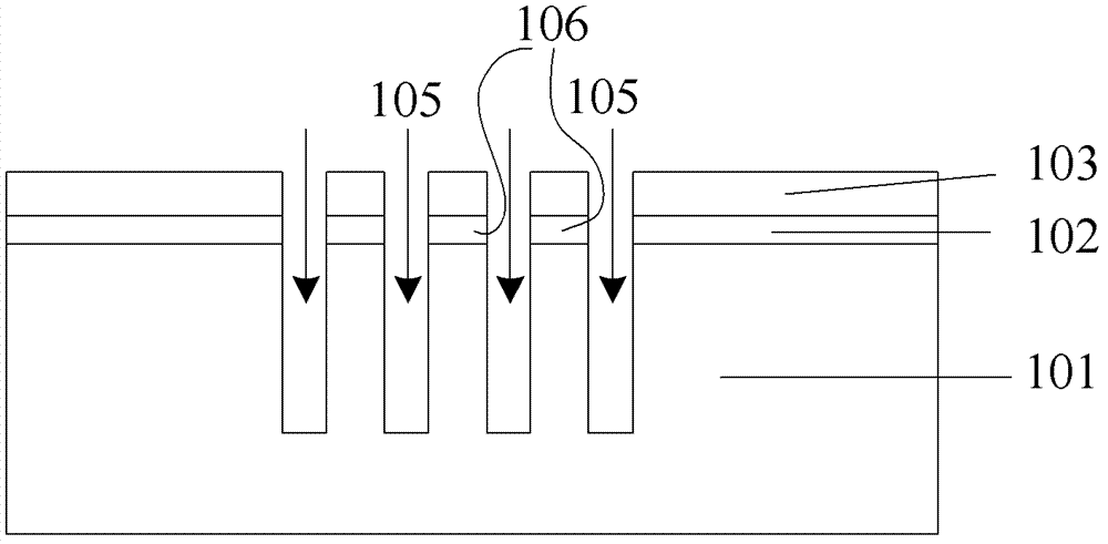
An embodiment of the invention discloses a high-density and embedded-type capacitor and a manufacturing method of the high density and embedded-type capacitor. The method comprises providing a base with a body layer and an etching barrier layer, forming a plurality of grooves with good verticality and high depth-to-width ratios, doping body layer materials of the bottom side walls of the groove and body layer materials between adjacent groove to get a doping area of the capacitor in order to form a three-dimensional PN junction on the contact regions of the body layer and a doping region, and forming a first electrode and a second electrode of the capacitor, wherein the polarities of the first electrode and the second electrode are opposite, and are electrically insulated, the first electrode is placed on two sides of the doping area or the periphery of the doping area, and the second electrode is placed on the surface of the doping area. Because the dielectric layer of the capacitor is made of three-dimensional grooves, the effective area of the dielectric layer is much larger than of a dielectric layer of an ordinary capacitor. Therefore, capacitance density of the capacitor is improved, and the capacitor can simultaneously satisfy requirements of low frequency decoupling and high frequency decoupling.

Description

Technical field [0001] The invention relates to the technical field of semiconductor manufacturing, and more specifically, to a high-density embedded capacitor and a manufacturing method thereof. Background technique [0002] With the rapid improvement of the integration of various functional circuits and the need for miniaturization of functional modules and components, integrated passive technology has become a solution to replace discrete passive devices to achieve device miniaturization. In various typical circuits, 80% of the components are passive devices, which occupy nearly 50% of the area on the printed circuit board. In System-in-Package (SiP, or System-on-Package, SOP) technology, integrated passive technology can be used to embed or integrate different passive devices or passive modules on the substrate , Can greatly reduce the area of ​​the substrate, and become one of the methods to achieve effective system integration. Capacitors are the most common and most dist...

Claims


Application Information

Patent Timeline
Patent Type & Authority Applications(China)
IPC IPC(8): H01L21/02H01L29/92
Inventor 王惠娟万里兮
Owner NAT CENT FOR ADVANCED PACKAGING
Learn More