
Super-junction schottky oxide pin diode having thin P-type layers under the schottky contact

a super-junction schottky oxide and pin diode technology, applied in the direction of basic electric elements, electrical equipment, semiconductor devices, etc., can solve the problems of low forward and reverse losses, high switching losses, forward voltage and low reverse current, etc., to achieve low forward voltage, low reverse current, and favorable switching performance

Active Publication Date: 2017-02-21
ROBERT BOSCH GMBH
View PDF7 Cites 0 Cited by
  • Summary
  • Abstract
  • Description
  • Claims
  • Application Information

AI Technical Summary

Benefits of technology

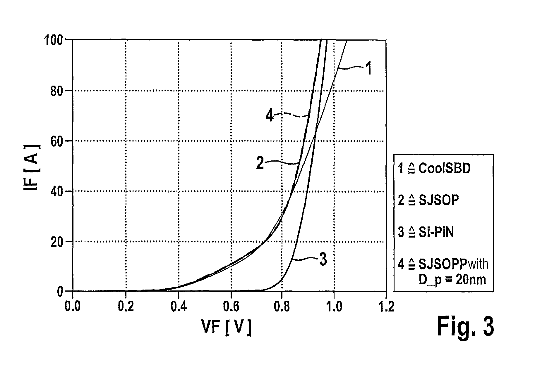
The patent is for a high-voltage diode that combines the properties of a Schottky diode and a PIN diode to create a super-junction structure. This diode has low forward voltage, good switching performance, and low reverse current. It includes thin, lightly doped layers that partially shield the Schottky contact, reducing reverse currents without affecting forward voltage or switching losses. Compared to other PIN power diodes, the SJSOPP has significantly lower switching losses at low forward voltages. It also has similar reverse currents and switching losses as a conventional SJSOP.

Problems solved by technology

PIN diodes exhibit low forward voltages and low reverse currents and, consequently, low forward and reverse losses.
However, high switching losses, which occur as switching-off losses during the commutation of the current, are disadvantageous.
A higher depletion current means a higher switching-off power loss.
In the case of PIN diodes, switching times and switching losses are high.
However, thick and lightly doped semiconductor layers are again necessary for high reverse voltages, which, in the case of high currents, results in unacceptable, high forward voltages.
Therefore, in spite of good switching performance, power Schottky diodes manufactured using silicon technology are not suitable for reverse voltages over approximately 100 V.
However, the low forward voltage of the PIN diode is not obtained at high currents.
However, upon de-energization, the minority carriers must also be swept out again with detrimental effects on the switching time.

Method used


Image

  • Super-junction schottky oxide pin diode having thin P-type layers under the schottky contact
  • Super-junction schottky oxide pin diode having thin P-type layers under the schottky contact
  • Super-junction schottky oxide pin diode having thin P-type layers under the schottky contact

Examples


Embodiment Construction

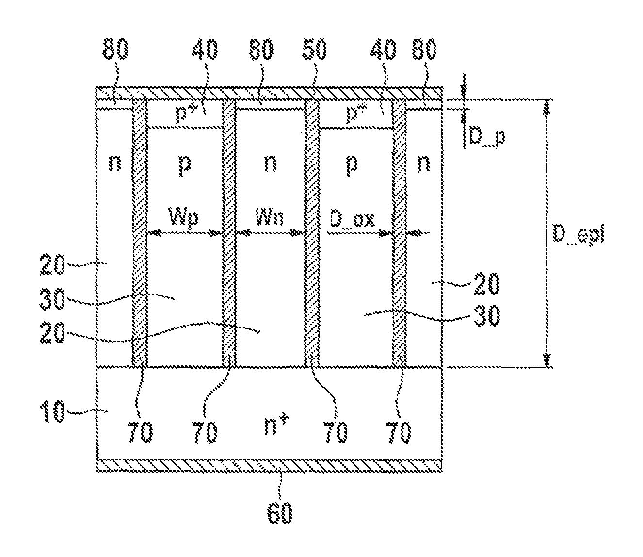
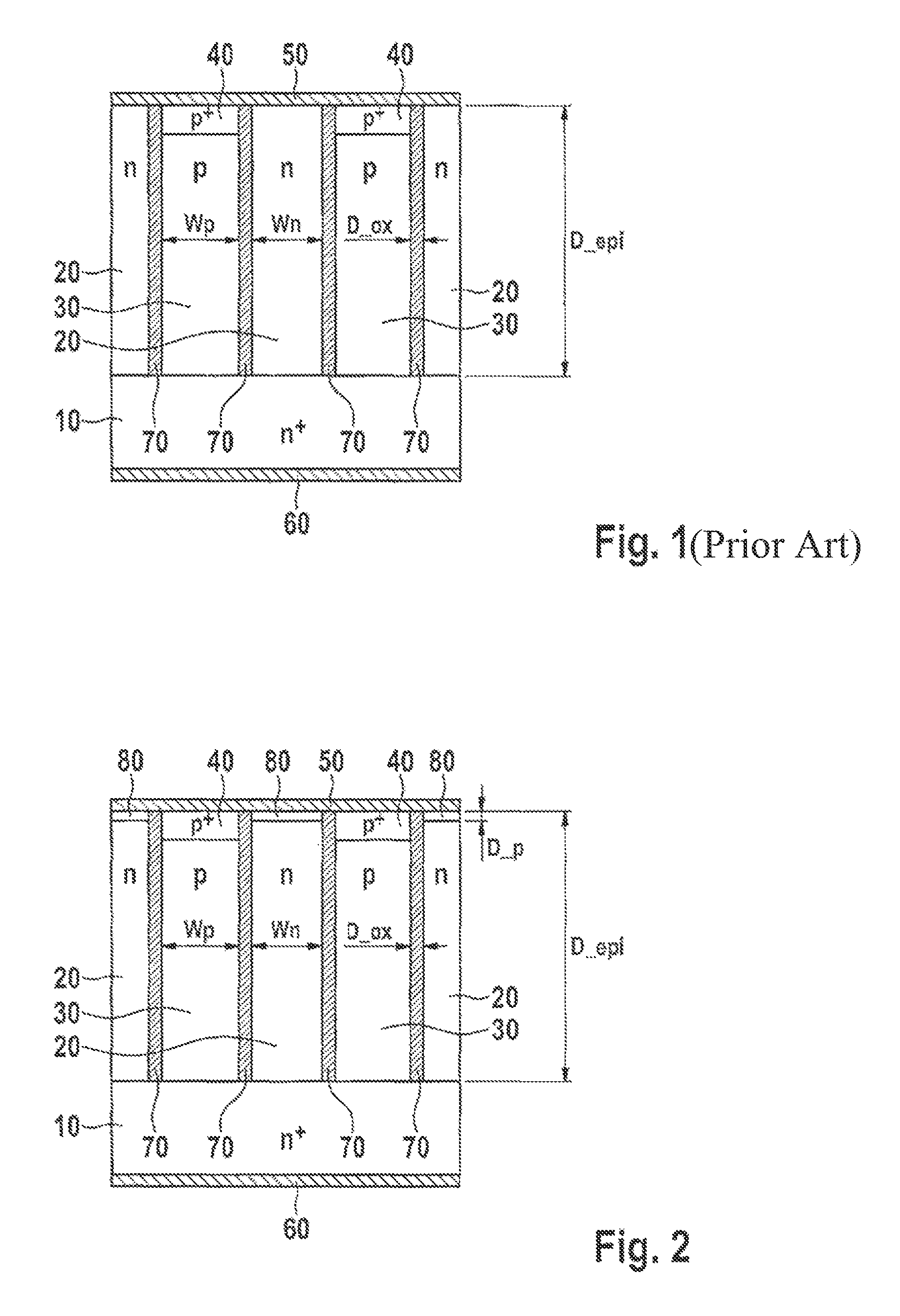
[0024]FIG. 2 shows a cross-sectional view of a detail of an example semiconductor chip according to the present invention, which is a super-junction Schottky oxide PIN diode having thin p-type layers under the Schottky contact. In the following, such a diode is always referred to as a SJSOPP. A SJSOPP is made up of an n+-type substrate 10, on which an n-type epitaxial layer 20 of thickness D_epi is situated. The n-type epitaxial layer 20 includes etched-in trenches 30, which are filled with p-type silicon and are filled with p+-type silicon 40 on the upper side. The width of n-type regions 20 is Wn, and that of p-type and p+-type regions 30 and 40 is Wp. The dopant concentrations and widths are selected so that the super-junction principle applies. Dielectric layers 70, which are preferably SiO2 layers having a thickness Dox, are provided between the p / p+-type and n-type regions. In this manner, the p-type and n-type regions are galvanically separated from one another.

[0025]A metall...


PUM


Abstract

A semiconductor chip, which includes an n-type substrate, over which an n-type epitaxial layer having trenches introduced into the epitaxial layer and filled with p-type semiconductor is situated, the trenches each having a heavily doped p-type region on their upper side, the n+-type substrate being situated in such a manner, that an alternating sequence of n-type regions having a first width and p-type regions having a second width is present; a first metallic layer, which is provided on the front side of the semiconductor chip, forms an ohmic contact with the heavily doped p-type regions and is used as an anode electrode; a second metallic layer, which is provided on the back side of the semiconductor chip, constitutes an ohmic contact and is used as a cathode electrode; a dielectric layer provided, in each instance, between an n-type region and an adjacent p-type region, as well as p-type layers provided between the n-type regions and the first metallic layer.

Description

CROSS REFERENCE[0001]The present application claims the benefit under 35 U.S.C. §119 of German Patent Application No. DE 102012201911.1 filed on Feb. 9, 2012, which is expressly incorporated herein by reference in its entirety.BACKGROUND INFORMATION[0002]Within the scope of the topic of CO2, increasingly efficient current converters are needed. Examples include inverters for photovoltaic or automotive applications. High-level blocking, low-loss and rapidly-switching power semiconductors are necessary for this. Apart from active semiconductor switches, such as IGBT's or CoolMOS transistors, free-wheeling diodes are also necessary. Generally, PIN diodes made of silicon are used for high-voltage applications. PIN diodes exhibit low forward voltages and low reverse currents and, consequently, low forward and reverse losses. However, high switching losses, which occur as switching-off losses during the commutation of the current, are disadvantageous.[0003]High-voltage PIN diodes are PN d...

Claims


Application Information

Patent Timeline
Patent Type & Authority Patents(United States)
IPC IPC(8): H01L29/872H01L29/06H01L29/868
CPCH01L29/872H01L29/0634H01L29/868H01L29/0649
Inventor QU, NINGGOERLACH, ALFRED
Owner ROBERT BOSCH GMBH
Learn More