
Fabrication of surface textures by ion implantation for antireflection of silicon crystals

a technology of surface texture and silicon crystals, applied in the direction of photovoltaics, electrical appliances, semiconductor devices, etc., can solve the problem of not being able to suppress achieve the effect of suppressing light reflection from si, small aspect ratio, and low packing density

Active Publication Date: 2016-01-05
THE RES FOUND OF STATE UNIV OF NEW YORK
View PDF16 Cites 0 Cited by
  • Summary
  • Abstract
  • Description
  • Claims
  • Application Information

AI Technical Summary

Benefits of technology

The invention is about a device made of crystalline silicon that prevents the reflection of light between 400 and 900 nm. This can reduce the amount of light that is lost when making certain types of devices. The invention can be used with current semiconductor technologies, making it a cost-effective solution for producing solar cells.

Problems solved by technology

Modification to crystalline Si surfaces by hydrogen [H] ion implantation is a well known phenomenon, but the surface structures generated by H implantation alone, typically of a low packing density and small aspect ratio, are not effective in suppressing light reflection from Si.

Method used


Image

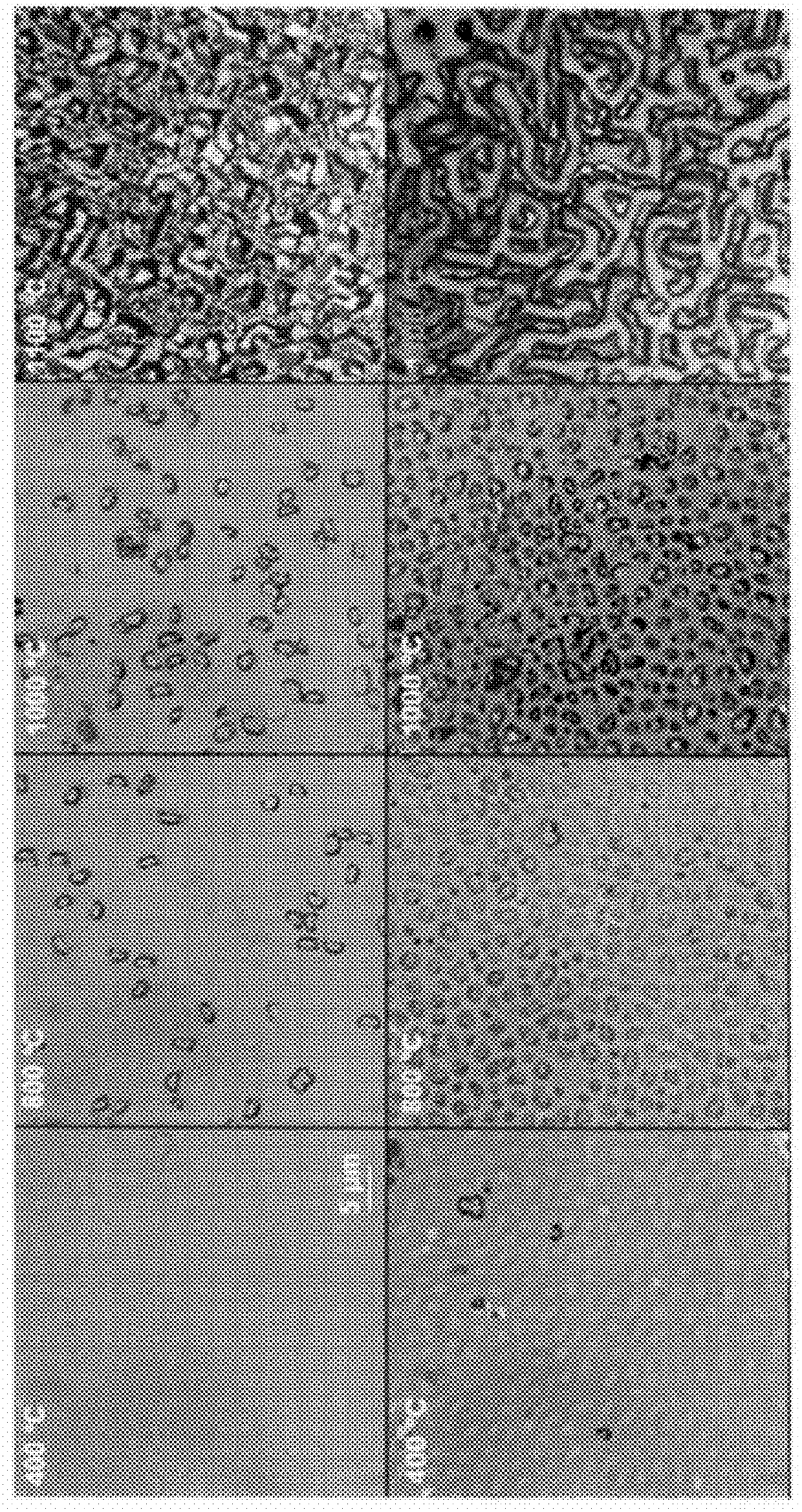
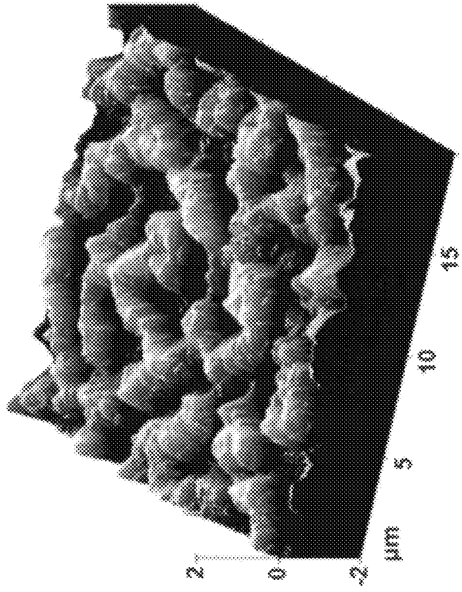
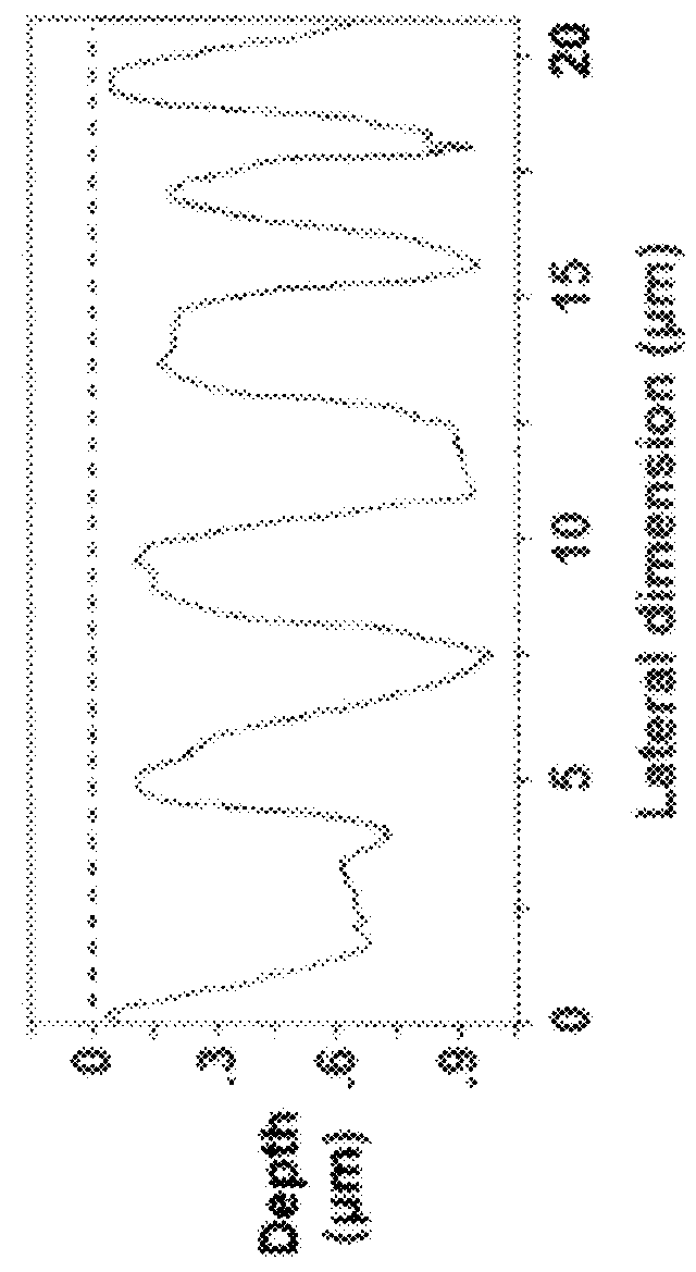
  • Fabrication of surface textures by ion implantation for antireflection of silicon crystals
  • Fabrication of surface textures by ion implantation for antireflection of silicon crystals
  • Fabrication of surface textures by ion implantation for antireflection of silicon crystals

Examples


Embodiment Construction

[0023]In a first aspect, the invention relates to a method for producing a textured crystalline silicon surface. A crystalline silicon substrate is provided. The crystalline silicon substrate can be single crystalline, polycrystalline or multicrystalline. These silicon substrates are especially suitable for use in solar cells. The crystalline silicon substrate can be a layer of silicon alone. In addition, the substrate may also be a silicon thin film, as in a silicon-on-insulator. The substrate may also be a polycrystalline silicon thin film of various grain size prepared on a separate substrate. In some instances, the crystalline silicon substrate may also be of either p- or n-type doping. A solar-grade silicon material could contain many impurity atoms, such as oxygen, carbon, and transition metals. These so-called p-type (e.g., boron) or n-type (e.g., phosphorus) are introduced intentionally in silicon solar cell fabrication, and they are needed to form a p-n junction for collect...


PUM

PropertyMeasurementUnit
temperatureaaaaaaaaaa

Abstract

The invention relates to a new method of texturing silicon surfaces suited for antireflection based on ion implantation of hydrogen and heavy ions or heavy elements combined with thermal annealing or thermal annealing and oxidation. The addition of the heavy ions or heavy elements allows for a more effective anti-reflective surface than is found when only hydrogen implantation is utilized. The methods used are also time- and cost-effective, as they can utilize already existing semiconductor ion implantation fabrication equipment and reduce the number of necessary steps. The antireflective surfaces are useful for silicon-based solar cells.

Description

CROSS-REFERENCE TO RELATED APPLICATIONS[0001]This application claims priority under 35 U.S.C. §119 to U.S. Provisional Application No. 60 / 406,452, filed Oct. 25, 2010, which is herein incorporated by reference in its entirety.BACKGROUND OF THE INVENTION[0002]1. Technical Field[0003]The present invention generally relates to textured crystalline silicon surfaces and methods of producing them. More particularly, the present invention relates to textured crystalline solar cells and methods of their fabrication.[0004]2. Background Information[0005]A critical step toward an enhanced efficiency in sunlight-to-electricity conversion through photovoltaic action is to minimize the reflection of sunlight from the surface of solar devices. This is of particular importance for solar cells based on silicon [Si] crystals, the dominant material in today's photovoltaic market. Si has a high refractive index, causing the reflection of more than 35% of infrared-to-ultraviolet light from a polished Si...

Claims


Application Information

Patent Timeline
Patent Type & Authority Patents(United States)
IPC IPC(8): H01L29/34H01L31/18H01L31/0236
CPCH01L29/34H01L31/02363Y02E10/50
Inventor HUANG, MENGBINGKADAKIA, NIRAGNACZAS, SEBASTIANBAKHRU, HASSARAM
Owner THE RES FOUND OF STATE UNIV OF NEW YORK
Learn More