Graphene based field effect transistor
a graphene-based field effect transistor and transistor technology, applied in the field of graphene-based semiconductor devices, can solve problems such as particularly challenging, and achieve the effects of low leakage current, high capacitance, and efficient and uniform seeding ald growth
- Summary
- Abstract
- Description
- Claims
- Application Information
AI Technical Summary
Benefits of technology
Problems solved by technology
Method used
Image
Examples
example 1
Device Fabrication
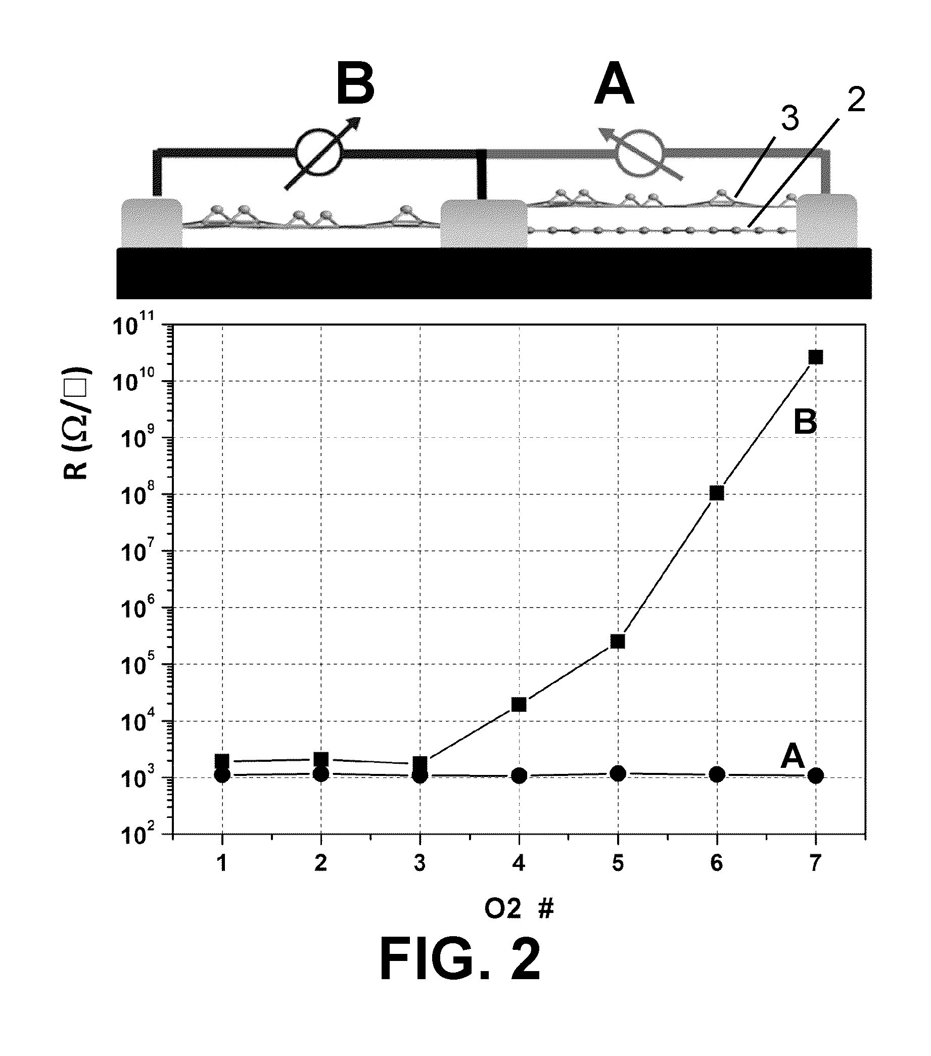
[0076]Reference is now made to FIG. 2.
[0077]Both samples A and B were formed on the same substrate (4).
[0078]Preparation of sample B:
[0079]A single layer graphene (SLG) flake (2) was deposited by micromechanical exfoliation on an n-doped Si substrate (4) covered with a 90 nm thermally grown SiO2 film, thereby forming sample B.
[0080]Preparation of sample A:
[0081]A single layer graphene (SLG) flake (2) was deposited by micromechanical exfoliation on an n-doped Si substrate (4) covered with a 90 nm thermally grown SiO2 film.
[0082]A large graphene film was then grown on copper thin film via Chemical Vapor Deposition (CVD). This film was then isolated from the copper foil and transferred onto the SiO2-supported graphene flake (2) by the standard polymethyl-methacrylate (PMMA) transferring method, thereby forming a substrate-double-layer graphene stack (sample A).
[0083]Standard photolithography was then performed on both sample A and sample B to (i) pattern samples A and...
example 2
Electrical Characterization
[0085]The resistances of samples A and B were measured after each plasma exposure / annealing step.
[0086]FIG. 2 compares the resistance of A and B versus the number of plasma exposure pulses.
[0087]The resistance of sample A was relatively constant while the resistance of sample B exponentially increased to 1011Ω.
[0088]Sample B (CVD graphene) changed to high resistance (insulator) upon oxidation.
[0089]The almost-constant resistance observed for sample A (stack of exfoliated single layer graphene (SLG) & CVD graphene) indicates that the underlying (metallic) SLG remains intact once the top layer (CVD graphene) undergoes oxidation.
[0090]We now refer to FIG. 3.
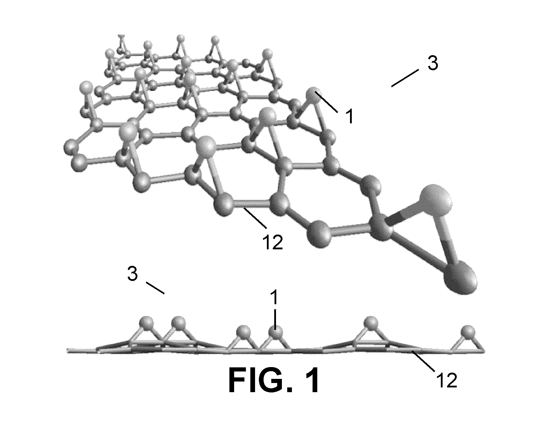
[0091]The most discussed feature in Raman spectra of graphene is the so-called 2D peak around 2700 cm−1, which is attributed to a two-phonon intervalley Raman scattering process. In the case of single layer graphene, the 2D peak consists of a single peak due to the presence of a single valence and conducta...
example 3
Top Date Stack Fabrication
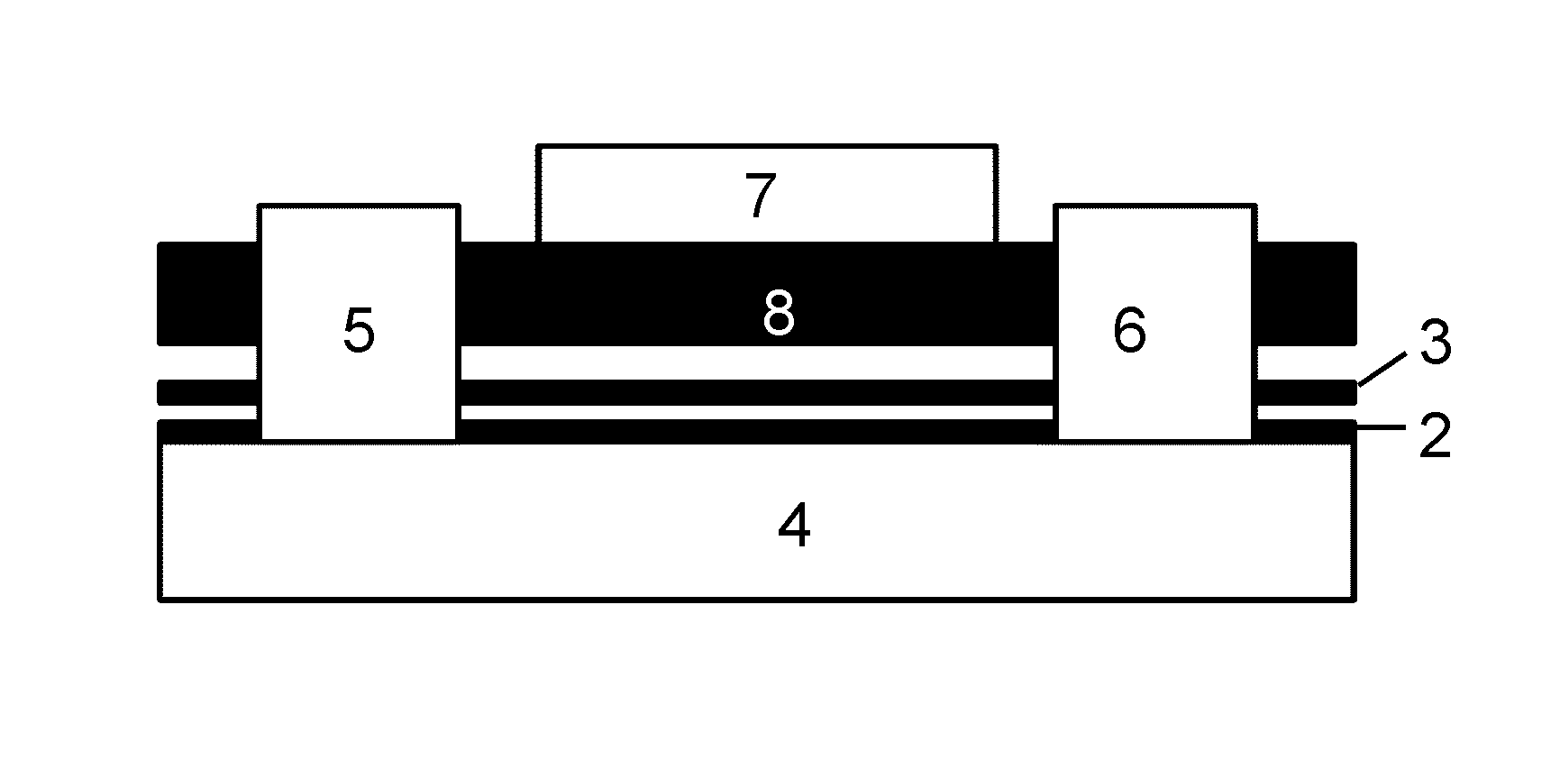
[0092]A 30 nm Al2O3 layer was deposited by ALD on the oxygen rich surface of sample 1 at 150° C. using alternate pulses of trimethylaluminum (TMA) and water. The dual-gate FET fabrication was then completed by fabricating a top-gate electrode by e-beam lithography (1 nm / 50 nm Cr / pd). FIG. 4 shows a schematic representation of a dual-gated FET with a graphene 2-graphene oxide 3 stack, wherein the graphene 2 is the channel and ALD-Al2O3 is grown on the graphene oxide 3.
[0093]FIG. 5 shows the transfer characteristics (Resistance R vs top-gate voltage (VTG)) of the dual-gated FET of example 3 at different voltages. It demonstrates that the source-drain resistance can be modulated with the device obtained in example 3.
[0094]FIG. 4 shows a Field effect transistor according to embodiments of the present disclosure. It comprises a semiconductor substrate 4 bearing a graphene layer 2 and a graphene oxide layer 3. It further comprises a high-k dielectric layer 8 on t...
PUM
| Property | Measurement | Unit |
|---|---|---|
| optical band gap | aaaaa | aaaaa |
| thickness | aaaaa | aaaaa |
| thickness | aaaaa | aaaaa |
Abstract
Description
Claims
Application Information
 - R&D
- Intellectual Property
- Life Sciences
- Materials
- Tech Scout
- Unparalleled Data Quality
- Higher Quality Content
- 60% Fewer Hallucinations
Browse by: Latest US Patents, China's latest patents, Technical Efficacy Thesaurus, Application Domain, Technology Topic, Popular Technical Reports.
© 2025 PatSnap. All rights reserved.Legal|Privacy policy|Modern Slavery Act Transparency Statement|Sitemap|About US| Contact US: help@patsnap.com


