Structure for picking up a collector and method of manufacturing the same

a technology of heterojunction bipolar transistors and collectors, which is applied in the direction of transistors, semiconductor devices, electrical apparatus, etc., can solve the problems of affecting the rf power characteristics of the device, the difficulty of lowering the parasitic capacitance ccs, etc., and achieves the effect of reducing the saturation voltage drop of the device, and reducing the parasitic capacitan

Active Publication Date: 2015-09-08
SHANGHAI HUAHONG GRACE SEMICON MFG CORP
View PDF17 Cites 0 Cited by
  • Summary
  • Abstract
  • Description
  • Claims
  • Application Information

AI Technical Summary

Benefits of technology

[0008]The present invention overcomes the aforementioned drawback of the conventional structure by presenting a novel structure for picking up a collector region of a heterojunction bipolar transistor (HBT). The structure is capable of reducing a parasitic capacitance between the structure for picking up a collector region and the substrate. In addition, the present invention also provides a method of manufacturing the structure for picking up a collector region of a HBT.
[0014]As indicated above, in the structure of the present invention, the undoped polysilicon layer may serve as a depletion region between the doped polysilicon layer and the substrate under a reverse bias, and thereby may significantly reduce the parasitic capacitance between the doped polysilicon layer and the substrate. Moreover, as the doped polysilicon layer connecting the collector region and the collector electrodes has a doping concentration higher than the collector region, the series resistance of the collector region and hence the saturation voltage drop of the device can be greatly reduced, on the other hand, a good ohmic contact can be formed between the doped polysilicon layer and the collector electrodes.
[0015]Furthermore, the intermediate layer optionally formed between the undoped and doped polysilicon layers may prevent the impurity in the doped polysilicon layer from diffusing into the undoped polysilicon layer, thus the undoped polysilicon layer is substantially an intrinsic polysilicon, which is more favorable to serve as a depletion region between the doped polysilicon layer and the substrate under a reverse bias to reduce the parasitic capacitance between the doped polysilicon layer and the substrate.

Problems solved by technology

Nevertheless, this device has a drawback that, as each pseudo buried layer 103 is a doped region below the isolation structure 102 formed by performing an ion implantation process with a low energy and a high dose at bottom of a corresponding one of the trenches and has a shallow junction and a high doping concentration, it is difficult to lower the parasitic capacitance Ccs between the pseudo buried layer 103 and the substrate 101, and as a result, the RF power characteristics of the device will be affected.

Method used


Image

  • Structure for picking up a collector and method of manufacturing the same
  • Structure for picking up a collector and method of manufacturing the same
  • Structure for picking up a collector and method of manufacturing the same

Examples


Embodiment Construction

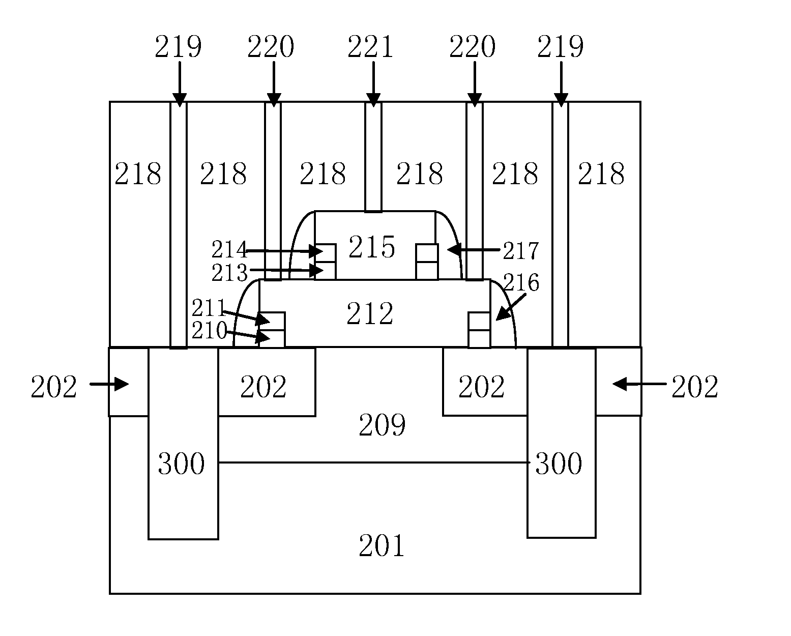
[0020]Referring to FIG. 2a, a structure for picking up a collector region of an ultra-high voltage SiGe HBT in accordance with embodiments of the present invention includes two polysilicon stacks 300 which are symmetrically formed in two isolation regions 202, and each of the polysilicon stacks 300 has a lower portion extending downward into a semiconductor substrate 201. The isolation regions 202 are located beneath a top surface of the substrate 201 for isolating an active region therebetween, namely the isolation regions 202 are symmetrically distributed on both sides of the active region.

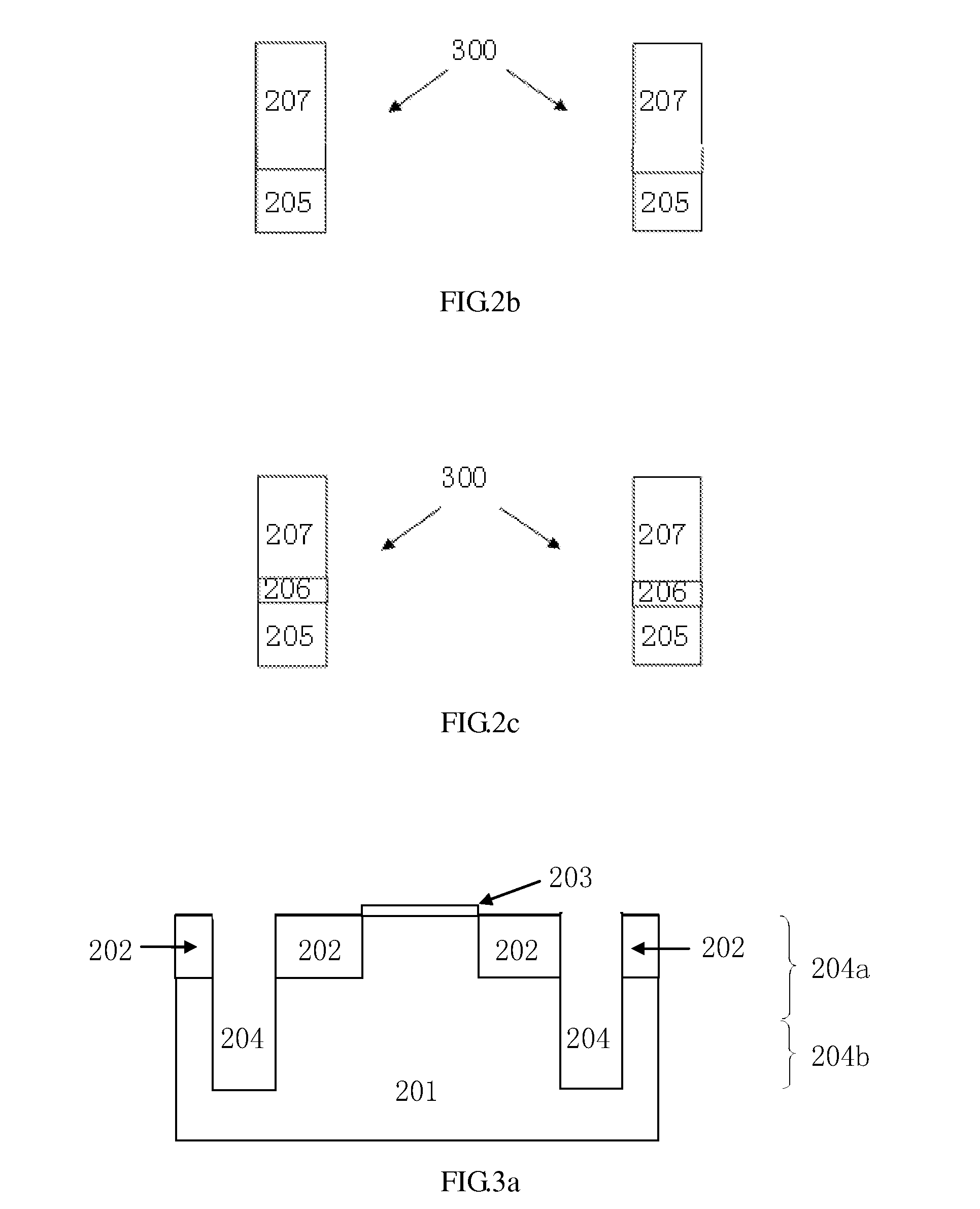
[0021]As shown in FIG. 2b, each polysilicon stack 300 comprises an undoped polysilicon layer 205 and a doped polysilicon layer 207 that is located on and in contact with the undoped polysilicon layer 205. The doped polysilicon layer has an opposite doping type to a conductivity type of the substrate 201. The collector region 209 is located between the two isolation regions 202 and also between t...


PUM


Abstract

A structure for picking up a collector region including a pair of polysilicon stacks formed in the isolation regions and extending below the collector region; and a pair of collector electrodes contacting on the polysilicon stacks, wherein the pair of polysilicon stacks includes: an undoped polysilicon layer and a doped polysilicon layer located on the undoped polysilicon layer, wherein a depth of the doped polysilicon layer is greater than a depth of the collector region; the depth of the collector region is greater than a depth of the isolation regions.

Description

CROSS-REFERENCES TO RELATED APPLICATIONS[0001]This application claims the priority of Chinese patent application number 201210163783.6, filed on May 23, 2012, the entire contents of which are incorporated herein by reference.TECHNICAL FIELD[0002]This disclosure pertains generally to a structure for picking up a collector region, and in particular, to a structure for picking up a collector region of a heterojunction bipolar transistor (HBT). The disclosure also relates to a method for manufacturing the structure for picking up a collector region.BACKGROUND[0003]Silicon-germanium (SiGe) is a semiconductor compound consisting of covalently bonded silicon and germanium atoms. It is a substitution solid solution of the two elements that can infinitely dissolve into each other. SiGe heterojunction bipolar transistors (HBTs) manufactured by using SiGe materials have become a kind of commonly used radio frequency (RF) devices.[0004]Chinese patent application Number 201110370460.X, entitled ...

Claims


Application Information

Patent Timeline
Patent Type & Authority Patents(United States)
IPC IPC(8): H01L29/732H01L29/73H01L29/08H01L29/737H01L29/66H01L21/763H01L29/417
CPCH01L29/73H01L29/0821H01L29/66234H01L29/66242H01L29/7378H01L21/763H01L29/41708
Inventor QIAN, WENSHENG
Owner SHANGHAI HUAHONG GRACE SEMICON MFG CORP
Why Eureka
Try Eureka