Pressure reconfigured electromagnetic devices
a technology of electromagnetic devices and reconfigurable wires, applied in the direction of instruments, conductive pattern formation, resonant antennas, etc., can solve the problems of bulky external control systems, inability to reconfigure the actual wires comprising the circuit, etc., and achieve the effect of less area
- Summary
- Abstract
- Description
- Claims
- Application Information
AI Technical Summary
Benefits of technology
Problems solved by technology
Method used
Image

Examples
example 1
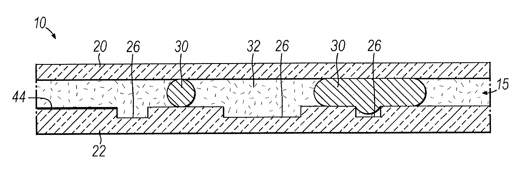
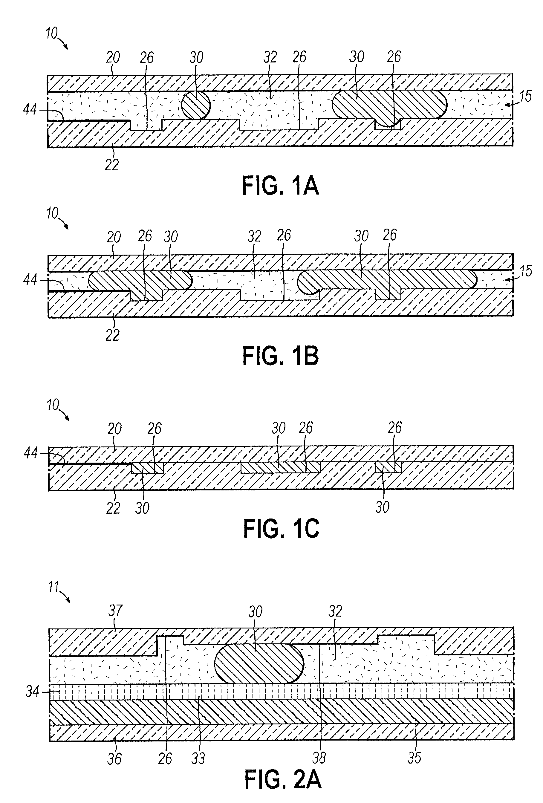
[0035]The device depicted in FIGS. 1A-1C was formed. It includes microreplicated channels 26 of 0.050 mm in thickness and various widths (0.050-1.0 mm) fabricated using a glass substrate and lamination of a negative-acting photoresist (DuPont PerMx). The substrate is placed onto a vacuum table then liquid metal is dosed onto the substrate a polymer sheet (polyethylene terephthalate) of 0.254 mm in thickness is then placed over top of the liquid metal and substrate. A 254 mm×254 mm sheet of pvc, 0.1 mm in thickness was placed over the entire device as well as the vacuum table stage to ensure a seal. The device as well as the space between the device and pvc layer is placed under vacuum at 9.8 psi and then returned to atmospheric pressure for the actuated and non-actuated states. This process can be repeated but for faster actuation by including a textile and a 0.03 mm thick polyimide track etched membrane with 0.0004 mm diameter vertical pores at a density of 1.5×1018 mm−2 (AR Brown-...
example 2
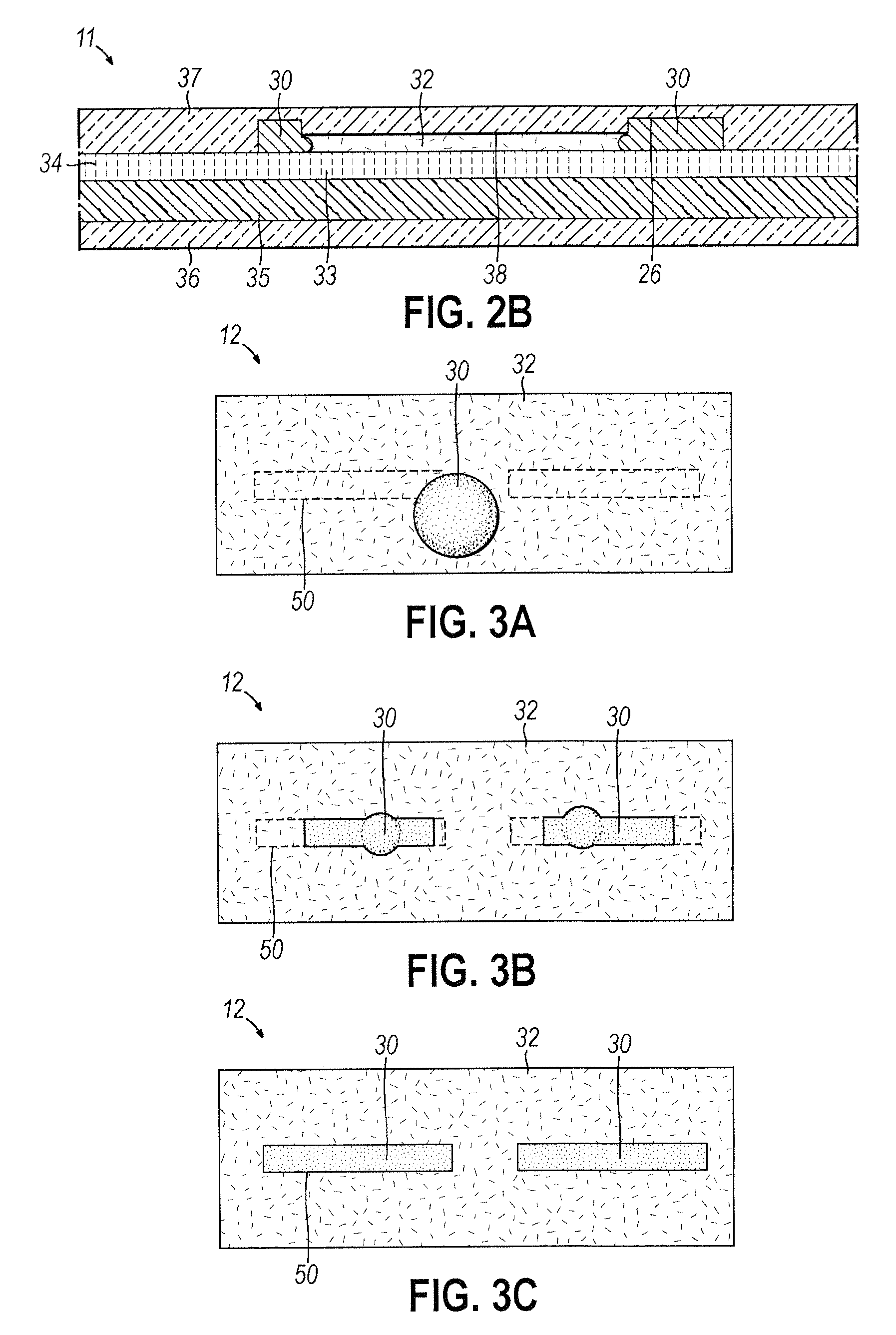
[0036]The device depicted in FIGS. 3A-3C is a switchable dipole antenna made according to the following example. Switchable dipole antenna 12 of 52 mm in length and approximately 0.5 mm in width was fabricated by laminating a polyimide tape (Kapton) of 0.15 mm in thickness onto a 0.254 mm polyethylene terephthalate substrate and then ablated using a CO2 laser to form trenches 50. Electrical traces (not shown) were made of silver ink, perpendicular to the dipole arms and extending ˜2.0 mm. Two via holes were ablated into another polyethylene terephthalate superstrate. Two copper leads (not shown) were attached to the silver ink traces. Liquid metal 30 and hydrochloric acid vapor 32 were located between the two layers. These leads were then attached to a network analyzer for resonance measurements while the device is in the on (resonant) (FIG. 3C) and off (non-resonant) (FIG. 3A) states. Distinct resonance frequencies were detected in only the on state.
example 3
[0037]A variable dipole fabrication. Fabrication of a mold for a pdms superstrate for the variable dipole antenna arm design was made by Makerbot Replicator 2 3D printer. The printed mold consists of two tapered dipole arms (˜1.0 mm taper in z direction) and retraction domes ˜4.0 mm in diameter. Double sided Kapton tape was cut into strips and placed on the edges of a porous track etched membrane. This allows for ease of realignment or refinement of the liquid metal dosed while still providing a durable seal with the final assembly. The liquid metal is dosed approximately to the size of the retraction domes of the pdms superstrate and placed on the membrane. The pdms and membrane strata are then pressed together forming a seal. A corner of the vacuum pouch is cut and a semi-rigid acid resistant tubing placed through this cut and applying epoxy around the tubing. Finally a textile wipe is inserted under the assembled dipole inside the vacuum pouch and a drop of HCl acid is placed ont...
PUM
| Property | Measurement | Unit |
|---|---|---|
| depth | aaaaa | aaaaa |
| thickness | aaaaa | aaaaa |
| thickness | aaaaa | aaaaa |
Abstract
Description
Claims
Application Information
 - R&D
- Intellectual Property
- Life Sciences
- Materials
- Tech Scout
- Unparalleled Data Quality
- Higher Quality Content
- 60% Fewer Hallucinations
Browse by: Latest US Patents, China's latest patents, Technical Efficacy Thesaurus, Application Domain, Technology Topic, Popular Technical Reports.
© 2025 PatSnap. All rights reserved.Legal|Privacy policy|Modern Slavery Act Transparency Statement|Sitemap|About US| Contact US: help@patsnap.com