Electron multiplier detector formed from a highly doped nanodiamond layer
a nanodiamond layer and detector technology, applied in the field of electromagnetic radiation or ion flow detection systems comprising electron multipliers in transmission, can solve the problems of low mechanical strength of diamond layers of such thicknesses, high cost of image intensifier tubes, and particularly long and complex tubes
- Summary
- Abstract
- Description
- Claims
- Application Information
AI Technical Summary
Benefits of technology
Problems solved by technology
Method used
Image
Examples
first embodiment
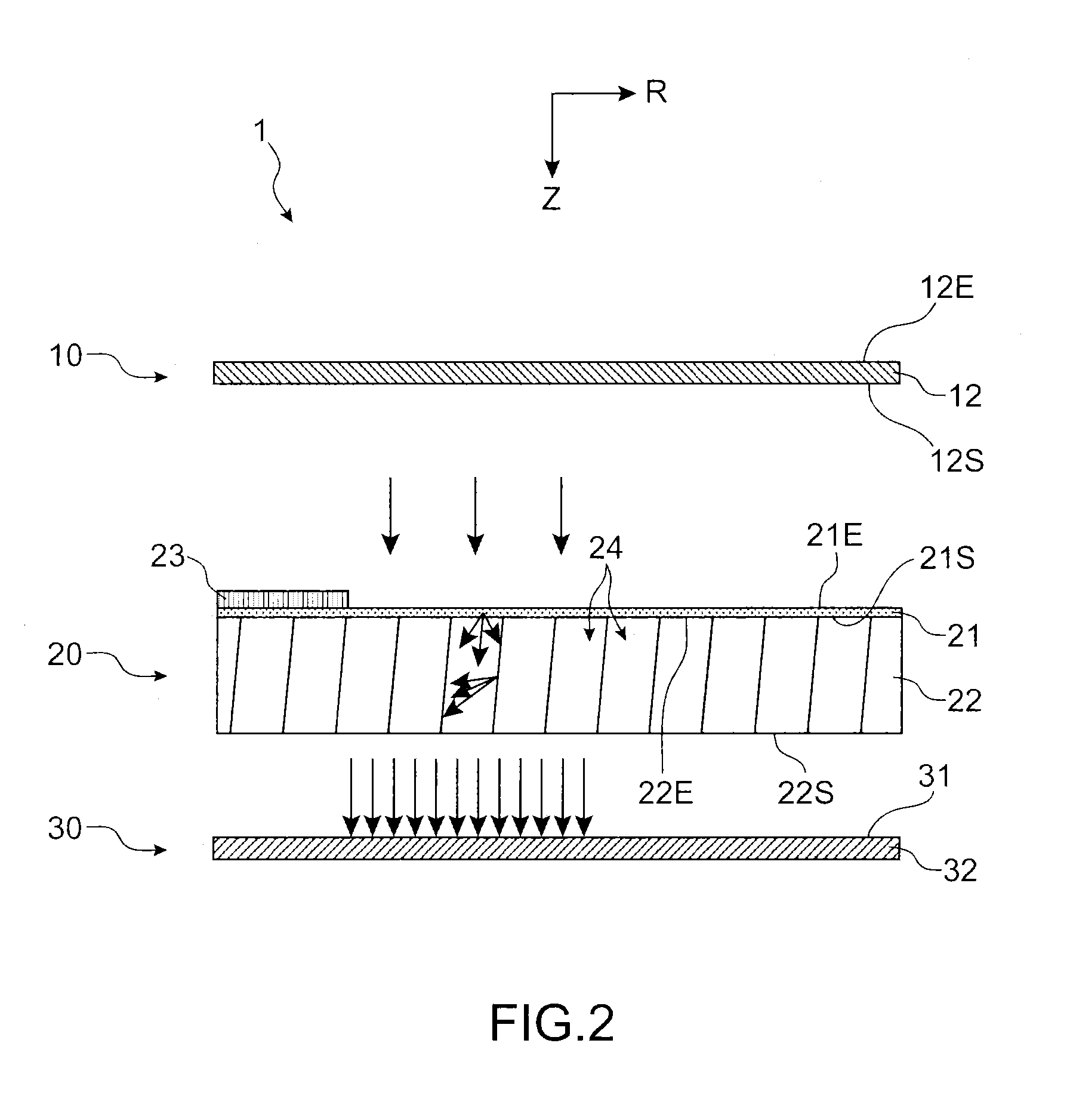
[0075]FIG. 2 illustrates partially and in a schematic manner an image intensifier tube according to the invention.
[0076]It should be noted that the scales are not respected in order to favour the clarity of the drawing.
[0077]Throughout the description that follows, an orthonormal mark (R,Z) in cylindrical coordinates is used where R is the radial direction of the tube and Z is the axial direction of the tube, which may also be substantially assimilated with the general direction of propagation of the electrons.
[0078]Furthermore, the terms “upstream” and “downstream” used hereafter should be understood herein in terms of orientation along the direction Z of the mark (R,Z).
[0079]In FIG. 2 is represented an image intensifier tube 1 according to the first embodiment of the invention. The tube 1 has a substantially cylindrical or tubular shape along the Z axis. However, the tube 1 may also have a square, rectangular, hexagonal section shape, or any other shape.
[0080]The tube 1 comprises ...
second embodiment
[0145]FIG. 4 is a partial schematic view of an image intensifier tube according to the invention.
[0146]Identical numerical references to those of FIG. 2 described previously designate identical or similar elements.
[0147]The image intensifier tube according to this embodiment differs essentially from the first embodiment described with reference to FIG. 2 in that the B-NCD diamond layer 21 is arranged between the MCP 22 and the output device 30, and in contact therewith.
[0148]It is thus not necessary to generate an electric field between the B-NCD diamond layer 21 and the output device 30.
[0149]The operation of the image intensifier tube according to this embodiment is similar to that of the tube described previously and is not described again here.
[0150]FIG. 5 is a partial schematic view of an image intensifier tube according to a variant of the second embodiment of the invention.
[0151]Identical numerical references to those of FIG. 4 described previously designate identical or simi...
third embodiment
[0160]FIG. 6 is a partial and schematic view of an image intensifier tube according to a
[0161]Identical numerical references to those of FIG. 2 described previously designate identical or similar elements.
[0162]The image intensifier tube according to this variant differs from the first embodiment described previously in that the electron multiplier no longer comprises a MCP but, quite the opposite, a plurality of B-NCD diamond layers 21 arranged one on another along the Z axis of the tube and spaced apart from each other.
[0163]The diamond layers may be arranged at a distance from each other comprised between several microns and several hundreds of microns, for example between 5 μm and 500 μm, and preferably between 30 μm and 500 μm, for example 50 μm.
[0164]As shown in FIG. 6, the collection electrode 23 may be arranged at the edge of the upstream face 21E of the diamond layer.
[0165]Alternatively, the collection electrode 23 of the upstream face 21E of each B-NCD diamond layer 21 may...
PUM
 Abstract
Description
Claims
Application Information
 - R&D
- Intellectual Property
- Life Sciences
- Materials
- Tech Scout
- Unparalleled Data Quality
- Higher Quality Content
- 60% Fewer Hallucinations
Browse by: Latest US Patents, China's latest patents, Technical Efficacy Thesaurus, Application Domain, Technology Topic, Popular Technical Reports.
© 2025 PatSnap. All rights reserved.Legal|Privacy policy|Modern Slavery Act Transparency Statement|Sitemap|About US| Contact US: help@patsnap.com


