Silicon-on-insulator substrate and fabrication method

a technology of silicon-on-insulator substrate and fabrication method, which is applied in the direction of basic electric elements, electrical apparatus, and semiconductor devices, can solve the problems of difficult to control the thickness of the top silicon layer by conventional methods, the thickness of the top silicon layer may be overly ground or polished, and the thickness of the top silicon layer may be difficult to achieve the effect of effectively controlling the thickness and surface roughness of the top silicon layer

Active Publication Date: 2015-03-17
SEMICON MFG INT (SHANGHAI) CORP
View PDF18 Cites 0 Cited by
  • Summary
  • Abstract
  • Description
  • Claims
  • Application Information

AI Technical Summary

Benefits of technology

[0008]The present disclosure provides an SOI substrate and a method for forming the SOI substrate to effectively control thickness and surface roughness of a top silicon layer of the SOI substrate.
[0011]Because the ion implanted layer is located in the first baseplate or the germanium-silicon layer, rather than located in the top silicon layer, the split of the first baseplate or the germanium-silicon layer do not affect the thickness of the top silicon layer, thus the thickness of the top silicon layer is easily to be controlled.
[0012]Further, the silicon-germanium layer joining the top silicon layer is removed in a wet etching process or a dry etching process with desired etch selectivity over the top silicon layer. The thickness of the top silicon layer and surface roughness of the first surface of the top silicon layer are easily to be controlled. This facilitates formation of semiconductor device(s) on the first surface of the top silicon layer.

Problems solved by technology

This may cause the semiconductor device to be scrapped.
However, it is difficult to control the thin thickness of the top silicon layer by conventional methods such as the smart cut process.
In addition, when grinding or polishing the surface of the top silicon layer using the chemical mechanical polishing process to reduce the surface roughness of the top silicon layer, the thin top silicon layer may be overly ground or polished and defects may occur when subsequently forming semiconductor devices on the ETSOI substrate.
The resulting semiconductor devices may thus be scrapped.

Method used


Image

  • Silicon-on-insulator substrate and fabrication method
  • Silicon-on-insulator substrate and fabrication method
  • Silicon-on-insulator substrate and fabrication method

Examples


Embodiment Construction

[0019]Reference will now be made in detail to exemplary embodiments of the disclosure, which are illustrated in the accompanying drawings. Wherever possible, the same reference numbers will be used throughout the drawings to refer to the same or like parts. For illustration purposes, elements illustrated in the accompanying drawings are not drawn to scale, which are not intended to limit the scope of the present disclosure. In practical operations, each element in the drawings has specific dimensions such as a length, a width, and a depth.

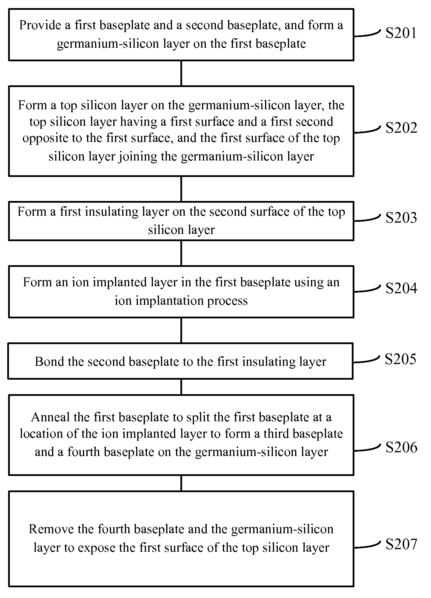
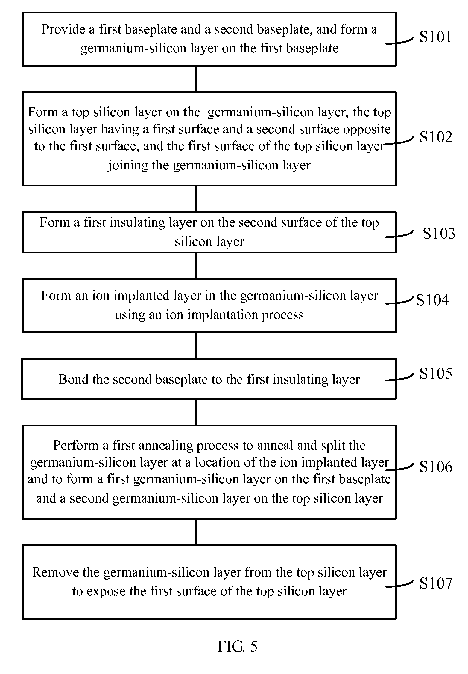
[0020]An SOI substrate and a method for forming the SOI substrate are provided to effectively control thickness and surface roughness of a top silicon layer of the SOI substrate.

[0021]For example, an SOI substrate can be formed by providing a first baseplate and a second baseplate and forming a silicon-germanium layer on the first baseplate. A top silicon layer can be formed on the silicon-germanium layer, the top silicon layer having a first surfa...


PUM

PropertyMeasurementUnit
thicknessaaaaaaaaaa
temperatureaaaaaaaaaa
pressureaaaaaaaaaa

Abstract

An SOI substrate and a method for forming the SOI substrate are provided. An SOI substrate can be formed by forming a silicon-germanium layer on a first baseplate. A top silicon layer can be formed on the silicon-germanium layer. A first insulating layer can be formed on the top silicon layer. An ion implanted layer can be formed in one of the silicon-germanium layer and the first baseplate. A second baseplate can be bonded to the first insulating layer. A first annealing process can be performed to anneal and split the one of the silicon-germanium layer and the first baseplate at the ion implanted layer. The silicon-germanium layer can be removed from the top silicon layer to expose the top silicon layer and to form the SOI substrate comprising the first insulating layer formed between the top silicon layer and the second baseplate.

Description

CROSS REFERENCE TO RELATED APPLICATIONS[0001]This application claims priority to Chinese patent application No. 201210071755.1, filed on Mar. 16, 2012, and entitled “METHOD FOR FORMING SILICON ON INSULATOR SUBSTRATE”, the entire disclosure of which is incorporated herein by reference.FIELD OF THE DISCLOSURE[0002]The disclosure relates to semiconductor manufacturing technology and, more particularly, to a silicon-on-insulator (SOI) substrate and a method for forming the SOI substrate.BACKGROUND OF THE DISCLOSURE[0003]A Silicon on Insulator (SOI) substrate is used as a substrate for integrated circuit (IC) manufacturing. Compared with a bulk silicon substrate, the SOI substrate may provide the ICs with low parasitic capacitance, high integration density, low short channel effect and fast speed, and dielectric isolation between components in the ICs. Use of SOI substrates may eliminate the parasitic latch-up effect, which often occurs when a bulk silicon substrate is used.[0004]Current...

Claims


Application Information

Patent Timeline
Patent Type & Authority Patents(United States)
IPC IPC(8): H01L21/00H01L21/02H01L21/762H01L29/06
CPCH01L21/76254H01L29/0649H01L21/02002
Inventor CHEN, ARIES
Owner SEMICON MFG INT (SHANGHAI) CORP
Why Eureka
Try Eureka