Method for polishing edge of glass substrate of display panel

a technology of display panels and glass substrates, applied in the field of precision machining, can solve the problems of glass chips flying and attaching to a non-polished area, cleaning the glass substrate, and the inability to protect the non-polished area of the glass substrate from surface damage, so as to achieve the effect of improving operation efficiency, facilitating the operation, and effectively protecting the non-polished area from contamination

Inactive Publication Date: 2014-10-02
SHENZHEN CHINA STAR OPTOELECTRONICS TECH CO LTD
View PDF24 Cites 0 Cited by
  • Summary
  • Abstract
  • Description
  • Claims
  • Application Information

AI Technical Summary

Benefits of technology

[0008]An object of the present invention is to provide a method for polishing an edge of a glass substrate of a display panel, which is easy to carry out, can effectively protect a non-polished area from contamination and damage caused by glass chips, and can effectively improve operation efficiency.

Problems solved by technology

A conventional glass substrate edge polishing machine that is used to polish edges of a glass substrate often causes glass chips to fly and attach to a non-polished area.
Such a solution, however, can only clean the glass substrate and cannot protect the non-polished area of the glass substrate from surface damage, such as scraping, caused by the glass chips.

Method used


Image

  • Method for polishing edge of glass substrate of display panel
  • Method for polishing edge of glass substrate of display panel
  • Method for polishing edge of glass substrate of display panel

Examples


Embodiment Construction

[0046]To further expound the technical solution adopted in the present invention and the advantages thereof, a detailed description is given to a preferred embodiment of the present invention and the attached drawings.

[0047]Referring to FIGS. 4-6, the present invention provides a method for polishing edge of glass substrate of display panel, which comprises the following steps:

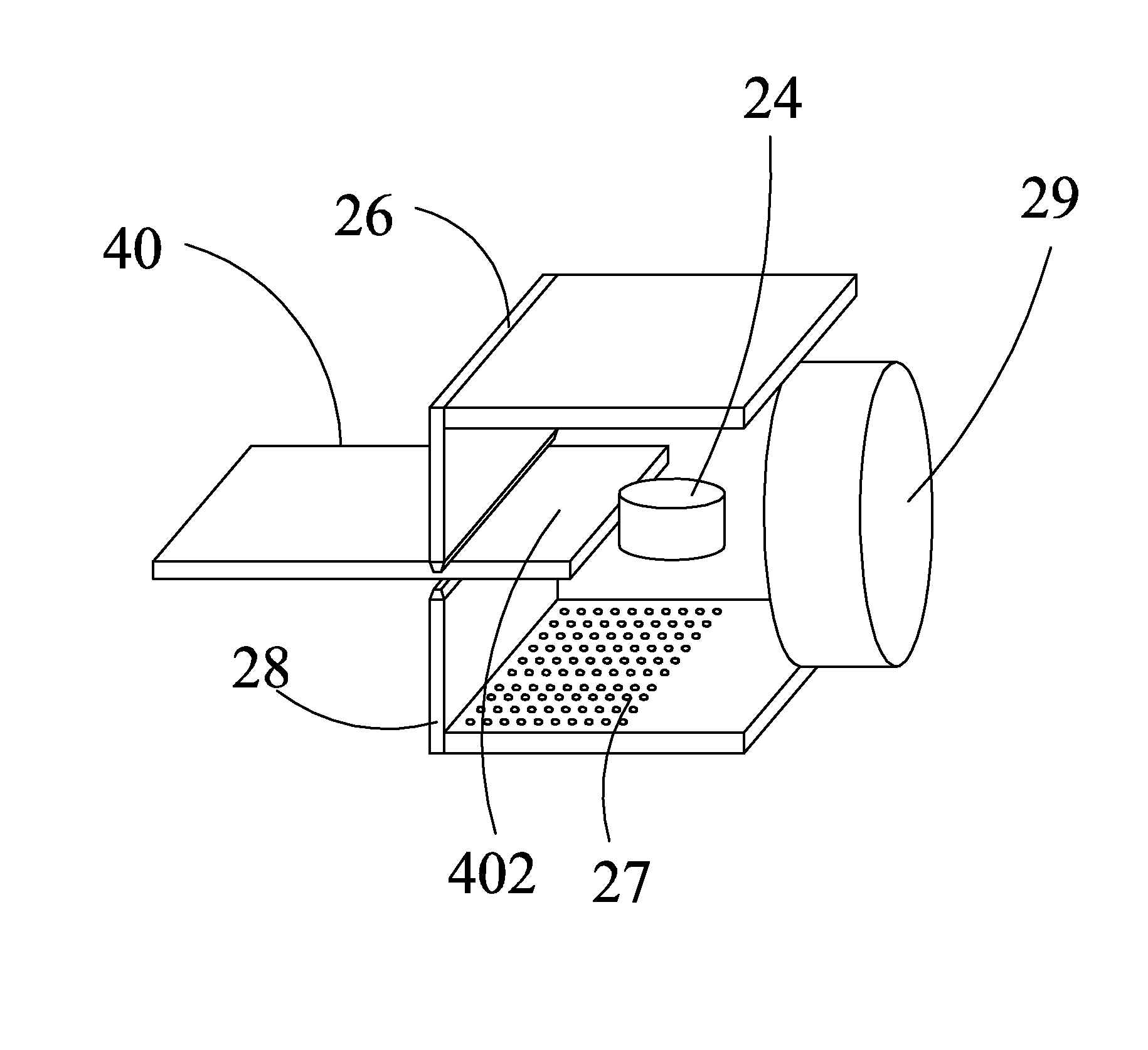
[0048]Step 1: conveying a glass substrate 40 of a display panel to be polished to a polishing device and positioning the glass substrate 40 for being subsequently polished by a grindstone 24 of the polishing device.

[0049]The glass substrate 40 comprises a polished area 402 and a non-polished area 404 located beside the polished area 402. The grindstone 24 of the polishing device is set in contact with the polished area 402. Step 1 can be carried out with any known technique and the polishing device can be a known device. The operation of positioning includes fixing the glass substrate 40 at a polishing positio...


PUM

PropertyMeasurementUnit
widthaaaaaaaaaa
elasticaaaaaaaaaa
transparent conductiveaaaaaaaaaa

Abstract

The present invention provides a method for polishing edge of glass substrate of display panel, which includes (1) conveying a glass substrate of a display panel to be polished to a polishing device and positioning the glass substrate for being subsequently polished by a grindstone of the polishing device; (2) providing first and second stop boards; (3) moving the first stop board to contact an upper surface of the glass substrate and moving the second stop board to contact a lower surface of the glass substrate; and (4) carrying out an edge polishing operation. By arranging the stop boards between the polished area and the non-polished area of the glass substrate, the glass chips generated during the polishing operation are prevented from flying and attaching to the surfaces of the non-polished area of the glass substrate during the polishing operation.

Description

BACKGROUND OF THE INVENTION[0001]1. Field of the Invention[0002]The present invention relates to the field of precision machining, and in particular to a method for polishing an edge of a glass substrate of a display panel.[0003]2. The Related Arts[0004]Flat panel displays have a variety of advantages, such as thin device body, low power consumption, and being free of radiation, and is thus widely used. The currently available flat panel displays include liquid crystal displays (LCDs) and organic light emitting display (OLEDs).[0005]Referring to FIG. 1, a conventional liquid crystal display device generally comprises a backlight module 100, a mold frame 300 arranged on the backlight module 100, a liquid crystal display panel 500 arranged on the mold frame 300, and a front bezel 700 arranged on the liquid crystal display panel 500. The backlight module 100 comprises a backplane 110, a backlight source 130 arranged in the backplane 110, a reflector plate 150 arranged in the backplane ...

Claims


Application Information

Patent Timeline
Patent Type & Authority Applications(United States)
IPC IPC(8): B24B9/10
CPCB24B9/10
Inventor CHEN, JIELEE, CHUNLIANGLO, CHANGCHENG
Owner SHENZHEN CHINA STAR OPTOELECTRONICS TECH CO LTD
Why Eureka
Try Eureka