Semiconductor device and process for producing the same

a technology of semiconductor devices and semiconductors, applied in semiconductor devices, semiconductor/solid-state device details, electrical apparatus, etc., can solve the problems of increasing resistance, insufficient contact hole opening formed by above etching, and increasing resistance, so as to effectively suppress the increase in resistance and occurrence

Inactive Publication Date: 2014-06-10
FUJITSU SEMICON LTD
View PDF34 Cites 0 Cited by
  • Summary
  • Abstract
  • Description
  • Claims
  • Application Information

AI Technical Summary

Benefits of technology

[0029]The first object of the present invention is to provide a semiconductor device being able to effectively suppress increase in resistance and occurrence of electric connection failure which can occur in a contact structure formed through a layer constituted by dividedly formed films.

Problems solved by technology

However, in the structures in which films (stressing films) for respectively applying predetermined stresses to channel regions in the nMOS substructure and the pMOS substructure are formed, problems occur as explained below.
However, when etching which causes overetching sufficient to remove the thick portion of the second stressing film 109 is performed, the portion of the silicide region 105 located under the bottom of the contact-hole formation region 112 (in particular, the portion of the silicide region 105 located under the first stressing film 107) is prone to etching damage, which can cause problems such as increase in the resistance.
The etching under the above etching condition cannot realize sufficient overetching in the region in which the first and second stressing films 107 and 109 overlap, so that the opening formed by the above etching becomes insufficient for being the contact hole.
As explained above, in the case where predetermined stressing films are dividedly formed over the nMOS substructure and pMOS substructure constituting a CMOS structure, and a contact hole is formed through the boundary between the stressing films, etching damage can occur in conductive regions such as a silicide region or a gate electrode located under the contact hole, or the contact hole (which extends to the conductive regions) can be imperfectly formed, so that the resistance increases or electric connection failure can occur.

Method used


Image

  • Semiconductor device and process for producing the same
  • Semiconductor device and process for producing the same
  • Semiconductor device and process for producing the same

Examples


first embodiment

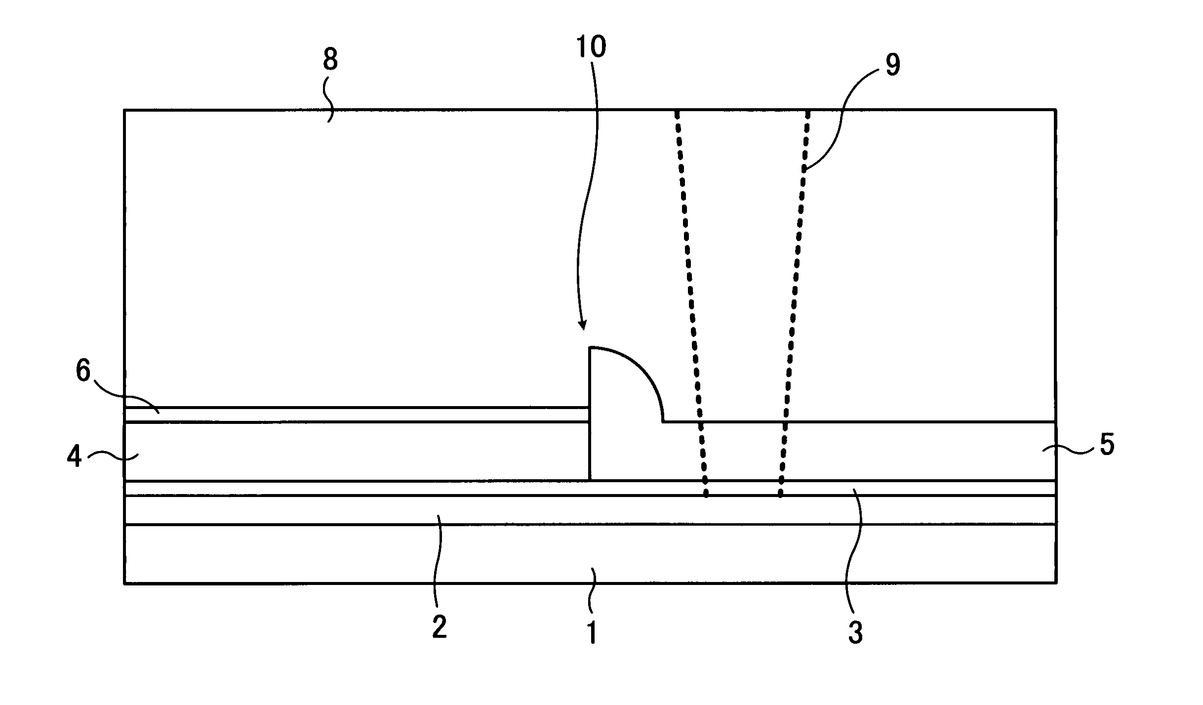
[0075]The semiconductor device according to the first embodiment of the present invention is explained below by taking a basic structure as an example. FIG. 1 is a schematic cross-sectional view of the basic structure of the semiconductor device according to the first embodiment. As illustrated in FIG. 1, the basic structure contains a contact structure in which a conductive region (made of a conductive material) is formed over different types of substructures (not shown), different films are dividedly formed in an upper layer located over the different types of substructures, and a contact electrode extending to the conductive region is formed.

[0076]For example, in the case of the CMOS inverter circuit in which an nMOS transistor and a pMOS transistor shares a gate electrode, and stressing films having different properties are dividedly formed over the nMOS transistor and the PMOS transistor in order to improve the device performance, a contact hole electrically connected to the ga...

second embodiment

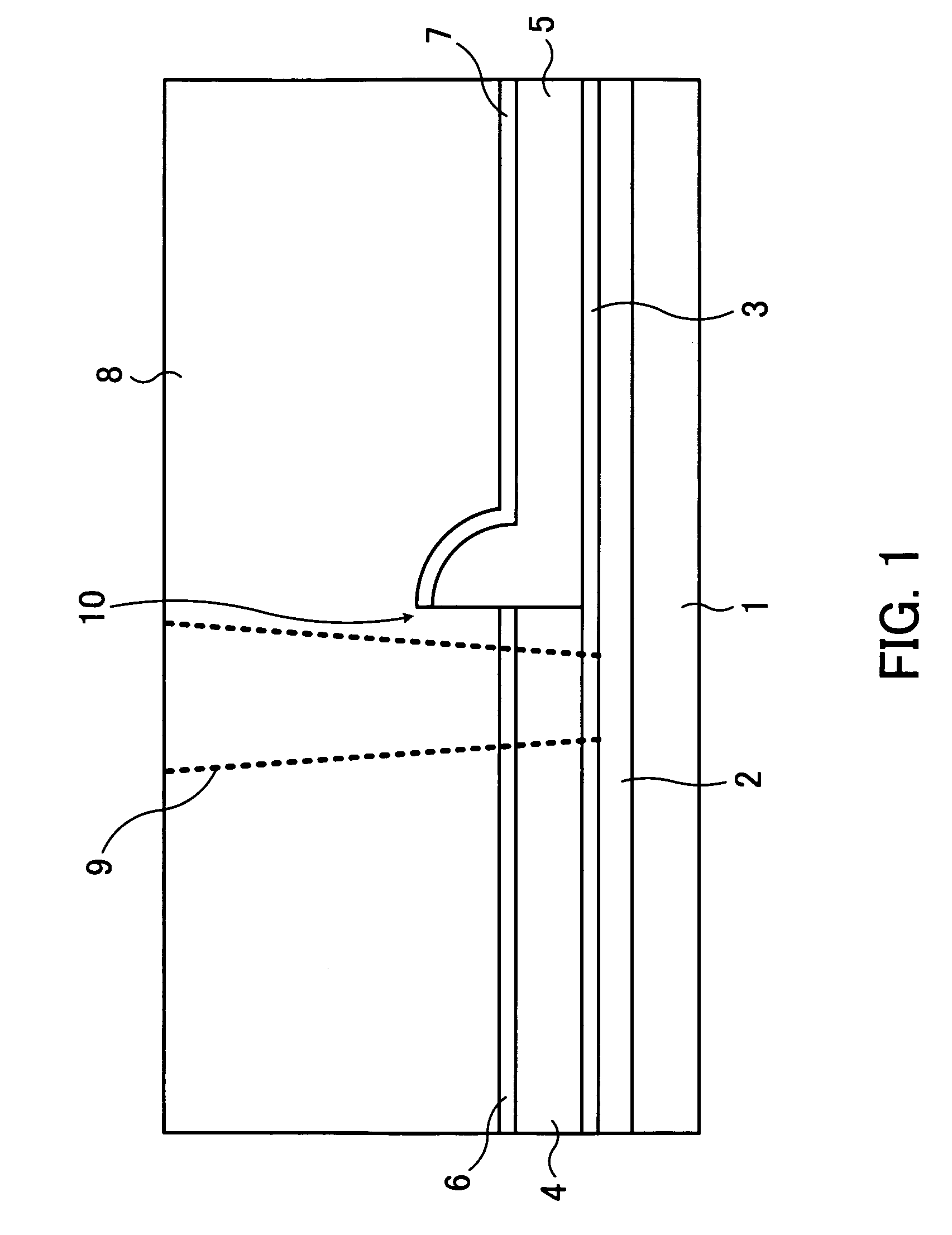
[0106]The semiconductor device according to the second embodiment of the present invention is explained below. FIG. 6 is a schematic cross-sectional view of the basic structure of a semiconductor device according to the second embodiment.

[0107]The semiconductor device according to the second embodiment illustrated in FIG. 6 is different from the first embodiment illustrated in FIG. 1 in that the contact-hole formation region 9 is arranged on the second-stressing-film side, where the second stressing film 5 is formed after the first stressing film 4 is formed. That is, the contact-hole formation region 9 and the division region 10 are arranged so that the contact-hole formation region 9 includes only the second stressing film 5 as a stressing film in the vicinity of the bottom of the contact-hole formation region 9 as indicated by the dashed lines in FIG. 6. For example, the contact-hole formation region 9 is arranged on the second-stressing-film side so as to avoid the thick portion...

third embodiment

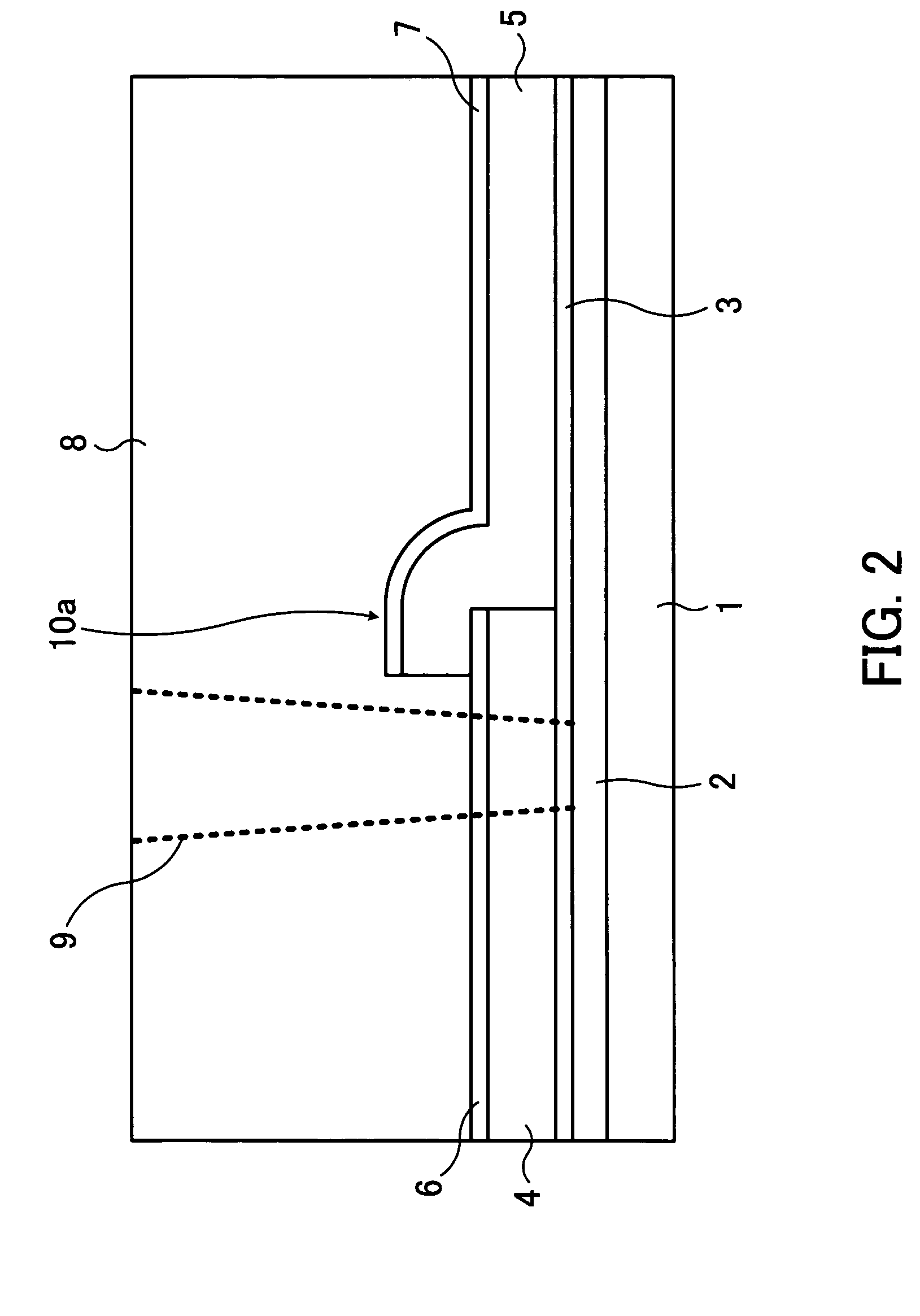
[0119]According to the first and second embodiments, the first, second, and third etching stopper films 3, 6, and 7 are used for dividedly forming the first and second stressing films 4 and 5, for example, as illustrated in FIGS. 1 and 6. According to the third embodiment of the present invention, the formation of at least a portion of the first, second, and third etching stopper films 3, 6, and 7 is dispensed with, as explained below.

[0120]FIGS. 11 to 13 are schematic cross-sectional views of the basic structures of the semiconductor devices according to the third embodiment. In the structures illustrated in FIGS. 11 to 13, the third etching stopper film 7 is not formed. Even in such structures, it is possible to arrange the contact-hole formation region 9 on the first-stressing-film side as illustrated in FIG. 11, or on the second-stressing-film side as illustrated in FIGS. 12 and 13. If the increase in the thickness of the second stressing film 5 in the boundary region is an amou...


PUM


Abstract

A semiconductor device having a contact structure is provided. The semiconductor device includes: a conductive region; a first film and a second film which are formed over the conductive region to realize a layer; and a contact electrode which extends through the layer to the conductive region, and is formed so as to replace a portion of the layer with a portion of the contact electrode, where the portion of the layer is constituted by only the first film, only the second film, or both of a portion of the first film and a portion of the second film, and the portion of the first film occupies a major part of the portion of the layer.

Description

CROSS-REFERENCE TO RELATED APPLICATIONS[0001]This application is based upon and claims the benefits of priority from the prior Japanese Patent Application No. 2006-058429, filed on Mar. 3, 2006, the entire contents of which are incorporated herein by reference.BACKGROUND OF THE INVENTION[0002]1) Field of the Invention[0003]The present invention relates to a semiconductor device having an interlayer contact structure, and to a process for producing the semiconductor.[0004]2) Description of the Related Art[0005]In the complementary MOS (Metal Oxide Semiconductor) field effect transistors (CMOSs) constituted by an n-channel MOS field effect transistor (nMOS) and a p-channel MOS field effect transistor (pMOS), it is desirable to increase the carrier mobility in each of the nMOS and pMOS transistors in order to speed up the nMOS and pMOS transistors.[0006]According to a conventional technique for increasing the carrier mobility, silicongermanium (SiGe) is used in a layer underlying a Si-...

Claims


Application Information

Patent Timeline
Patent Type & Authority Patents(United States)
IPC IPC(8): H01L23/48H01L29/78H01L23/52H01L21/8238H01L29/40
CPCH01L21/823864H01L21/823807H01L21/76877H01L29/7843H01L21/823871H01L2924/0002H01L2924/00
Inventor MORIOKA, HIROSHIOGURA, JUSUKEPIDIN, SERGEY
Owner FUJITSU SEMICON LTD
Why Eureka
Try Eureka