Method of semiconductor integrated circuit, and computer readable medium

a technology of integrated circuits and computer programs, applied in the direction of cad circuit design, program control, instruments, etc., can solve the problems of increasing the size of the semiconductor integrated circuit, increasing the length of the signal wiring passing through the functional macros, and increasing the wiring delay, so as to and suppress the increase of the wiring delay and the occurrence of timing errors

Inactive Publication Date: 2013-02-19
RENESAS ELECTRONICS CORP
View PDF15 Cites 1 Cited by
  • Summary
  • Abstract
  • Description
  • Claims
  • Application Information

AI Technical Summary

Benefits of technology

[0029]In the design method of the semiconductor integrated circuit according to the present invention, the area having apices of opposing corners of the position of the start point logic cell and the position of the end point logic cell is set to the repeater search area, and the repeater candidate is searched within this area. Accordingly, the repeater can be arranged in a position to make the signal wiring route between the start point logic cell and the end point logic cell the shortest, thereby suppressing an increase in the wiring delay and an occurrence of a timing error.
[0031]In the circuit design program according to the present invention, the area having apices of opposing corners of the position of the start point logic cell and the position of the end point logic cell is set to the repeater search area, the drive boundary is set based on the drive ability of the start point logic cell, and the repeater candidate is searched within this area. Accordingly, the repeater can be arranged in a position to make the signal wiring route between the start point logic cell and the end point logic cell the shortest, thereby making it possible to suppress an increase in the wiring delay and an occurrence of a timing error.
[0032]The present invention provides a design method of a semiconductor integrated circuit and a computer readable medium which are able to suppress an increase in a wiring delay and an occurrence of a timing error.

Problems solved by technology

An increase in functional macros in a semiconductor integrated circuit results in an increase in a size of the semiconductor integrated circuit and an increase in the length of a signal wiring passing through the functional macros, which increases the wiring delay.
Thus, it becomes difficult to achieve high-speed operation in the semiconductor integrated circuit.
Accordingly, it is impossible to satisfy the transfer rate that is required, and timing error occurs in the timing verification (step S109 in FIG. 14).
Thus, a bypass route of a redundant signal wiring is generated and the signal wiring is increased, which increases the wiring delay.
Hence, the wiring delay cannot be within the transfer rate that is required and timing error is occurred, so that the assignment of the wiring layer and inserting of the repeater need to be repeated.

Method used


Image

  • Method of semiconductor integrated circuit, and computer readable medium
  • Method of semiconductor integrated circuit, and computer readable medium
  • Method of semiconductor integrated circuit, and computer readable medium

Examples


first exemplary embodiment

[0048]Hereinafter, a first exemplary embodiment of the present invention will be described with reference to the drawings.

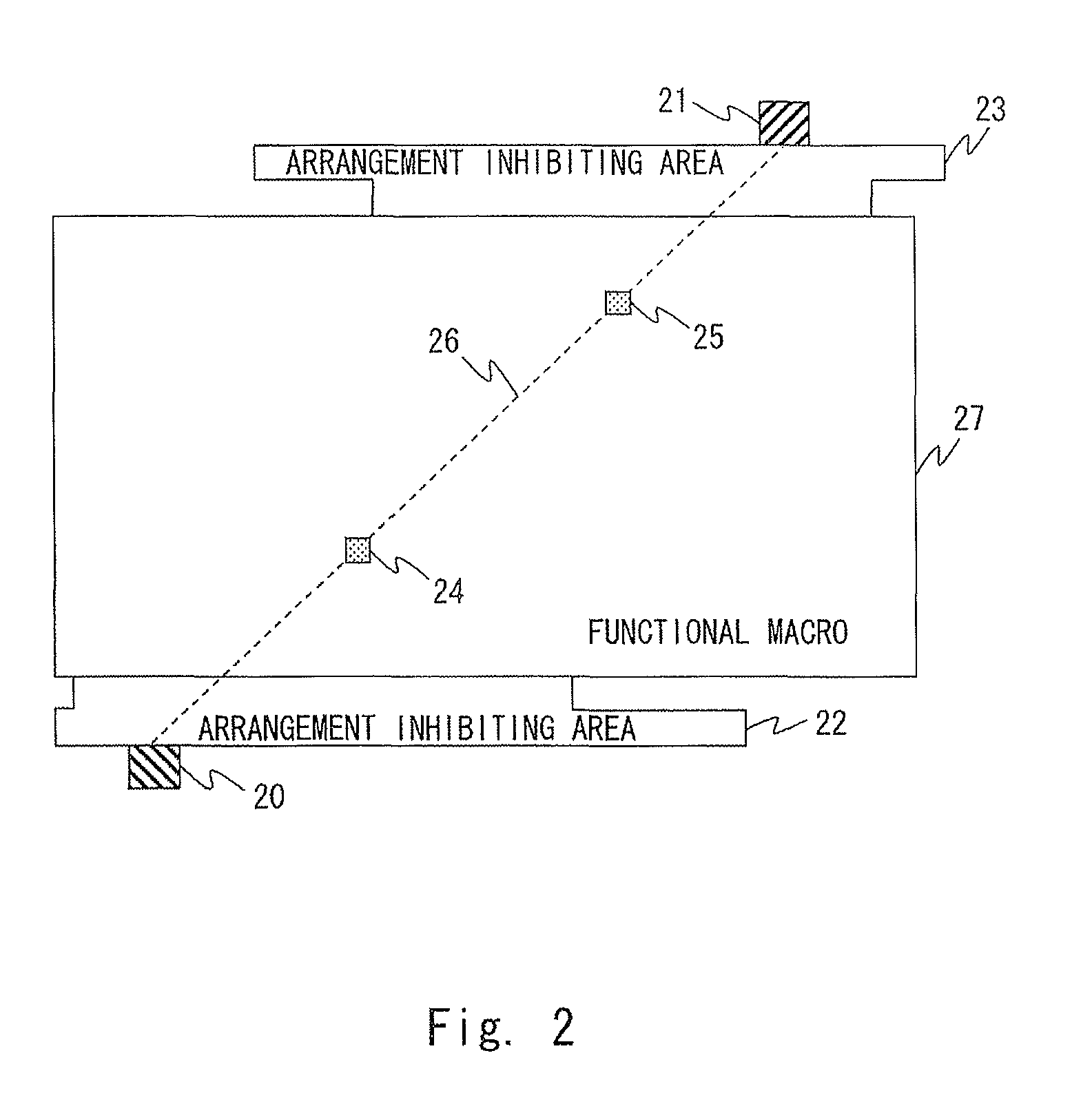
[0049]FIG. 2 is a diagram for describing a design method of a semiconductor integrated circuit according to the first exemplary embodiment. FIG. 2 shows a state in which repeaters 24 and 25 are initially arranged so that a signal wiring image 26 that connects a start point logic cell 20 and an end point logic cell 21 becomes the shortest when the signal wiring image 26 passes on a functional macro 27 and arrangement inhibiting areas 22 and 23.

[0050]FIG. 3 is a diagram for describing a case in which a repeater arrangement possible area is extracted using the design method of the semiconductor integrated circuit according to the first exemplary embodiment. FIG. 3 shows a repeater arrangement possible area from the state in which the start point logic cell 20, the end point logic cell 21, the functional macro 27, and the arrangement inhibiting areas 22 and 23 shown ...

second exemplary embodiment

[0094]Hereinafter, a second exemplary embodiment of the present invention will be described with reference to the drawings.

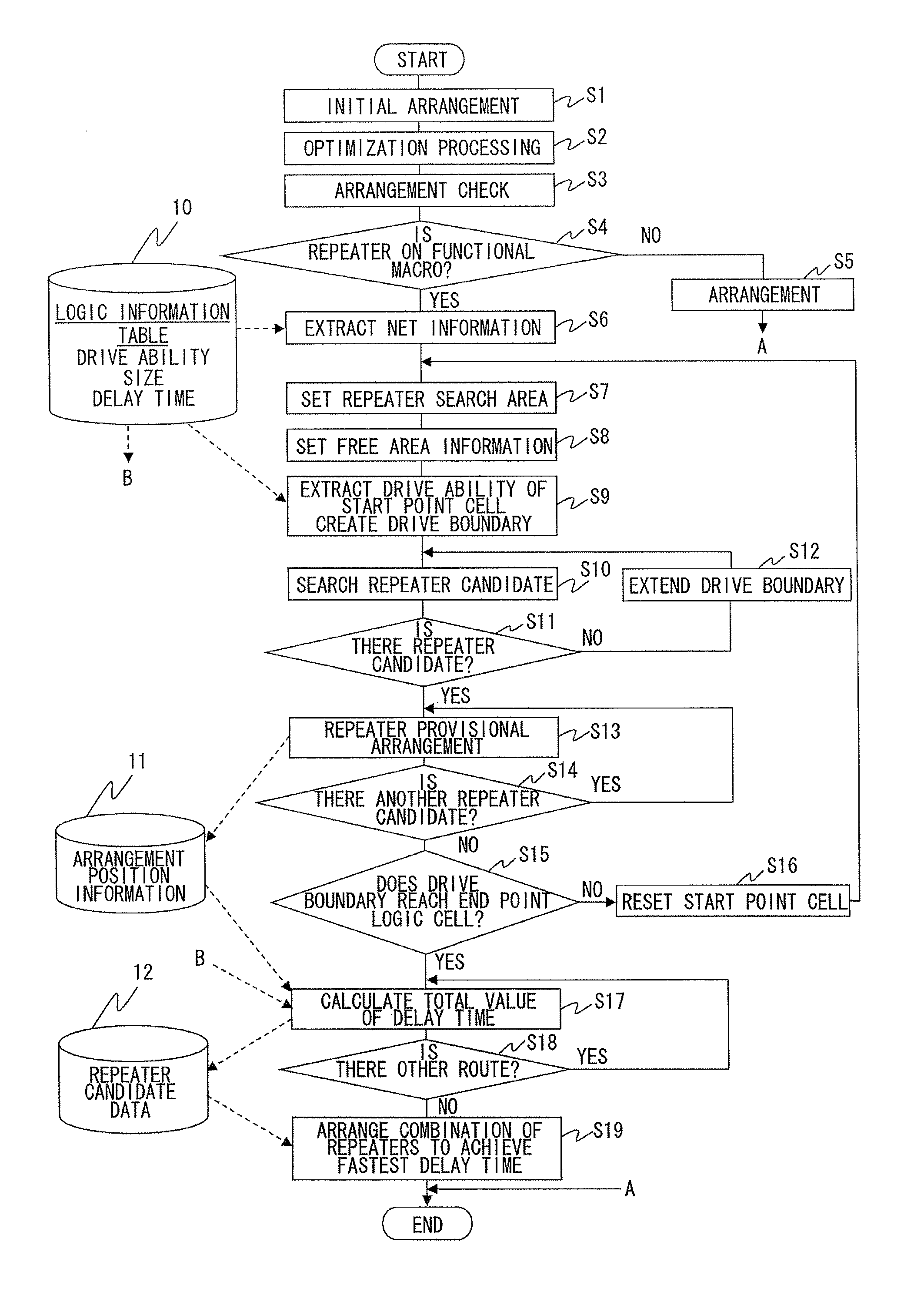
[0095]FIG. 10 is a flow chart for describing a design method of a semiconductor integrated circuit according to the second exemplary embodiment of the present invention. In the flow chart shown in FIG. 10, the step S7 in the flow chart shown in FIG. 1 is changed to step S7′. In the step S7′ in the flow chart shown in FIG. 10, a search area extension parameter 13 is externally input, so as to extend the repeater search area. The other processing is similar to that shown in FIG. 1, and thus description will be omitted.

[0096]FIG. 11 is a diagram for describing a case in which the repeater arrangement possible area is extracted using the design method of the semiconductor integrated circuit according to the second exemplary embodiment. FIG. 11 shows the repeater arrangement possible area from the arrangement state of the start point logic cell 20, the end point logi...


PUM


Abstract

A design method of a semiconductor integrated circuit sets an area having apices of opposing corners of a position of a start point logic cell and a position of an end point logic cell to a repeater search area, adds free area information to the repeater search area, sets a drive boundary in the repeater search area based on a drive ability of the start point logic cell, searches a repeater candidate that can be arranged in an area of the drive boundary based on the free area information, calculates a delay time from the start point logic cell to the end point logic cell based on delay time information and a coordinate of the repeater candidate that is searched, and determines a repeater arranged between the start point logic cell and the end point logic cell from the repeater candidate based on the delay time that is calculated.

Description

INCORPORATION BY REFERENCE[0001]This application is based upon and claims the benefit of priority from Japanese patent application No. 2009-292712, filed on Dec. 24, 2009, the disclosure of which is incorporated herein in its entirety by reference.BACKGROUND[0002]1. Field of the Invention[0003]The present invention relates to a design method of a semiconductor integrated circuit, and a computer readable medium, and more particularly, to a design method of a semiconductor integrated circuit and a computer readable medium that optimize the layout of the semiconductor integrated circuit.[0004]2. Description of Related Art[0005]There has been an increasing demand for an increase in a speed of a semiconductor integrated circuit including a system on chip (SoC) due to an increase in a speed of systems mounted thereon and an increase in a macro size as a result of complicated functions. To meet this demand, a logic synthesis method and an arrangement / wiring design method using various high...

Claims


Application Information

Patent Timeline
Patent Type & Authority Patents(United States)
IPC IPC(8): G06F17/50G06F9/455
CPCG06F17/5068G06F30/39
Inventor KONDOU, KEIICHIROUTSUCHIYA, HIROYUKI
Owner RENESAS ELECTRONICS CORP
Why Eureka
Try Eureka