Semiconductor device
a technology of semiconductor devices and display devices, applied in pulse generators, pulse techniques, instruments, etc., can solve the problems of delay, distortion, delay, delay, etc., and achieve the effect of reducing the rise time of an output signal from a circuit, reducing the power consumption of the circuit, and reducing the current flowing between the wirings of the circuit via the transistor
- Summary
- Abstract
- Description
- Claims
- Application Information
AI Technical Summary
Benefits of technology
Problems solved by technology
Method used
Image
Examples
embodiment 1
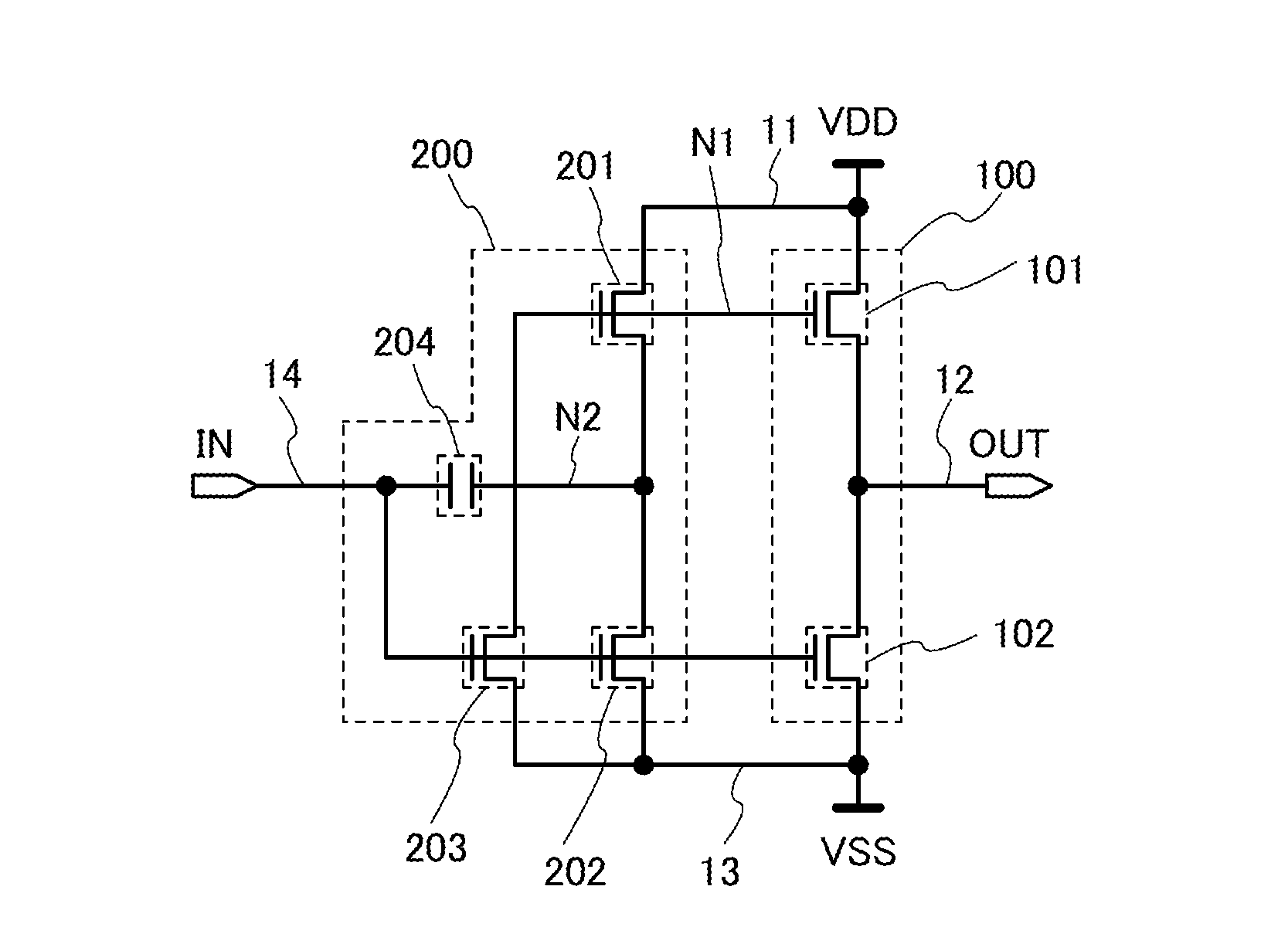
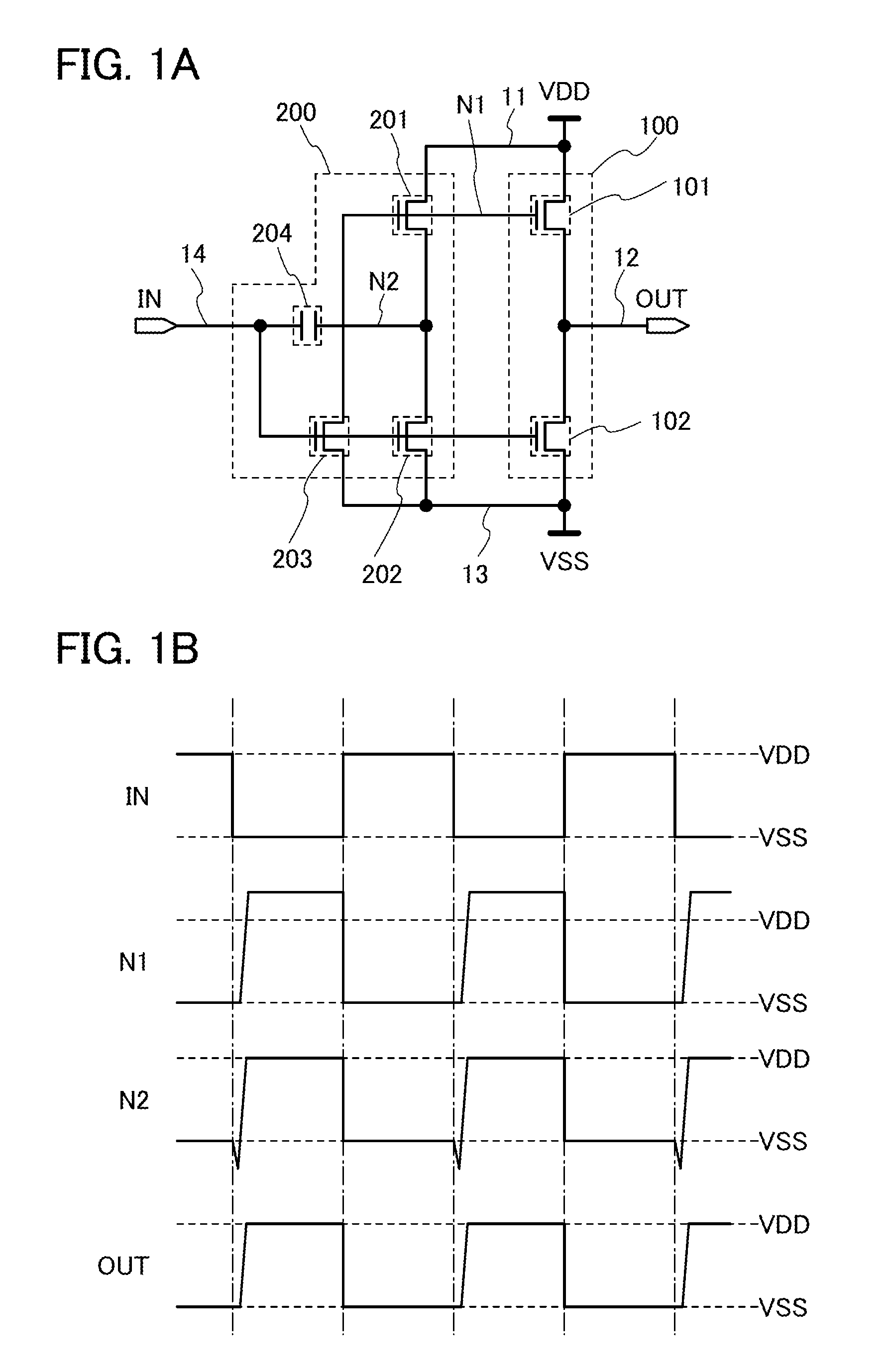
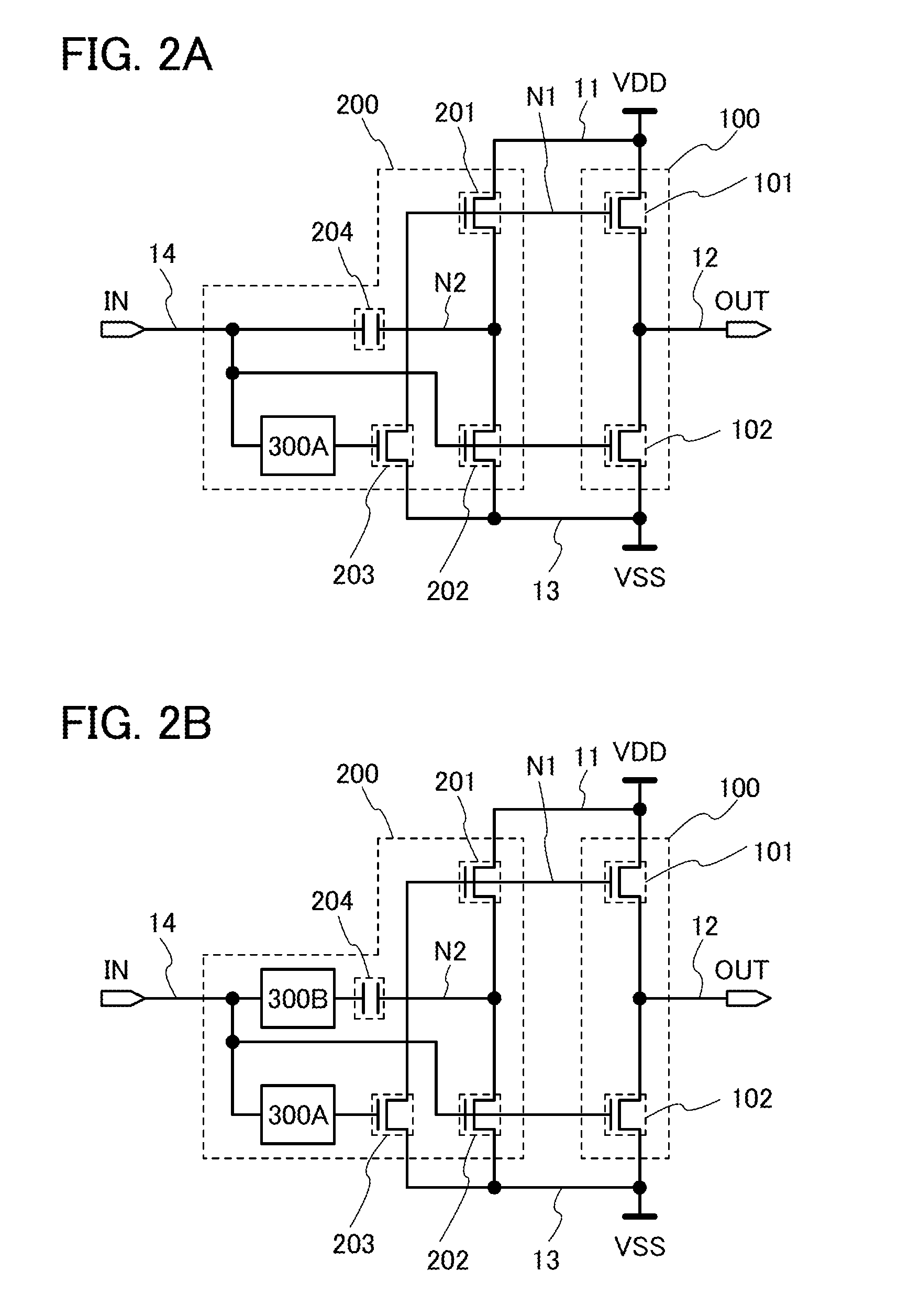
[0036]In Embodiment 1, an inverter circuit (also referred to as “semiconductor device” or “driver circuit”) according to one embodiment of the present invention will be described.
[0037]The configuration of an inverter circuit in this embodiment will be described with reference to FIG. 1A.
[0038]The inverter circuit illustrated in FIG. 1A includes a circuit 100 and a circuit 200. The circuit 100 is connected to a wiring 11, a wiring 12, a wiring 13, a wiring 14, and the circuit 200. The circuit 200 is connected to the wiring 11, the wiring 13, the wiring 14, and the circuit 100.
[0039]The circuit 100 includes a transistor 101 and a transistor 102. A first terminal (also referred to as “one of a source and a drain”) of the transistor 101 is connected to the wiring 11. A second terminal (also referred to as “the other of the source and the drain”) of the transistor 101 is connected to the wiring 12. A first terminal of the transistor 102 is connected to the wiring 13. A second terminal o...
embodiment 2
[0149]In Embodiment 2, a shift register circuit (also referred to as “semiconductor device” or “driver circuit”) according to one embodiment of the present invention will be described.
[0150]A shift register circuit in this embodiment includes a plurality of flip-flop circuits (also referred to as “semiconductor devices” or “driver circuits”). First, a flip-flop circuit will be described, and then a shift register circuit including the flip-flop circuit will be described.
[0151]A flip-flop circuit included in the shift register circuit of this embodiment will be described with reference to FIG. 7A.
[0152]The flip-flop circuit in FIG. 7A includes a transistor 401, a transistor 402, a transistor 403, a transistor 404, a transistor 405, and a circuit 500. A first terminal of the transistor 401 is connected to a wiring 21. A second terminal of the transistor 401 is connected to a wiring 22. A first terminal of the transistor 402 is connected to the wiring 13. A second terminal of the trans...
embodiment 3
[0234]Using an EL display device as an example, cross-sectional structures of a pixel and a driver circuit of a display device according to one embodiment of the present invention will be described with reference to FIG. 12. FIG. 12 exemplifies cross-sectional structures of a pixel 840 and a driver circuit 841.
[0235]The pixel 840 includes a light-emitting element 832 and a transistor 831 having a function of supplying current to the light-emitting element 832. In addition to the light-emitting element 832 and the transistor 831, the pixel 840 may also include a variety of semiconductor elements such as a transistor that controls input of an image signal to the pixel 840 and a capacitor that holds the potential of an image signal.
[0236]The driver circuit 841 includes a transistor 830 and a capacitor 833 for holding the gate voltage of the transistor 830. The driver circuit 841 corresponds to the inverter circuit in Embodiment 1 or the flip-flop circuit or the shift register circuit i...
PUM
 Abstract
Description
Claims
Application Information
 - R&D
- Intellectual Property
- Life Sciences
- Materials
- Tech Scout
- Unparalleled Data Quality
- Higher Quality Content
- 60% Fewer Hallucinations
Browse by: Latest US Patents, China's latest patents, Technical Efficacy Thesaurus, Application Domain, Technology Topic, Popular Technical Reports.
© 2025 PatSnap. All rights reserved.Legal|Privacy policy|Modern Slavery Act Transparency Statement|Sitemap|About US| Contact US: help@patsnap.com


