Semi-conductor substrate and method of masking layer for producing a free-standing semi-conductor substrate by means of hydride-gas phase epitaxy

a technology of semi-conductor substrate and mask layer, which is applied in the direction of non-metal conductors, instruments, oxide conductors, etc., can solve the problems of subsequent processing, failure to manufacture gan crystals with diameters of 2 inches or more by conventional single crystal growth, and failure to grow by means of sublimation, etc., to achieve the effect of increasing the thickness of the layer

Active Publication Date: 2013-11-26
FREIBERGER COMPOUND MATERIALS
View PDF27 Cites 1 Cited by
  • Summary
  • Abstract
  • Description
  • Claims
  • Application Information

AI Technical Summary

Benefits of technology

[0032]The process enables the manufacture of low-defect, free-standing GaN wafers, which self-separate from the starting substrate. This separation may occur already during the growth due to tensile stresses of the grown semiconductor layer increasing with increasing layer thickness, or yet at the latest by the different thermal expansion coefficients during the cooling from a growth temperature. It has been found that such a separation occurs particularly when using tungsten silicide nitride or tungsten silicide as the mask material. Therefore, an additional technological step for separation can be dispensed with. Due to separation already at high temperatures, the GaN wafers have only a low or no warping or bowing, which is advantageous for the further processing.

Problems solved by technology

Contrary to other semiconductors, e.g. silicon (Si) and gallium arsenide (GaAs), to date the manufacture of GaN crystals having diameters of 2 inch or more by means of conventional single crystal growth has been unsuccessful.
Up to now, growth by means of sublimation is unsuccessful, either.
This is disadvantageous, e.g. with respect to the achievable dislocation densities and the warping resulting from different lattice constants and differences in thermal expansion.
This warping partly also results in problems in the subsequent processing, because e.g. transfer of structures by means of photolithographic processes is limited on warped wafers in terms of resolution.
Thereby, a further process step is necessary, which is laborious and limited in yield for larger areas.
Furthermore, this process does not solve the problem of warping, since the package consisting of GaN-layer and -substrate is cooled from growth temperature to room temperature.
This process requires a laborious etching process for removing the GaAs substrate, which, moreover, is toxic.
However, it is unclear how the porosity of this TiN layer can be controlled, and whether this process can be performed in a reproducible manner.
This process however does not avoid warping of the package consisting of starting substrate and GaN layer.

Method used


Image

  • Semi-conductor substrate and method of masking layer for producing a free-standing semi-conductor substrate by means of hydride-gas phase epitaxy
  • Semi-conductor substrate and method of masking layer for producing a free-standing semi-conductor substrate by means of hydride-gas phase epitaxy
  • Semi-conductor substrate and method of masking layer for producing a free-standing semi-conductor substrate by means of hydride-gas phase epitaxy

Examples


first embodiment

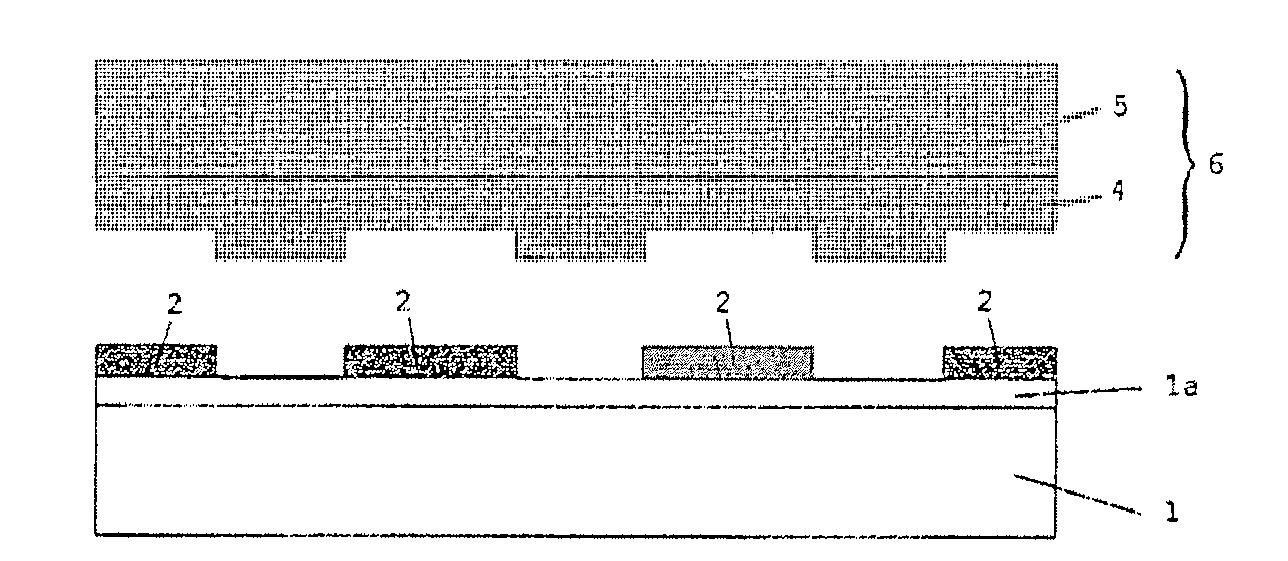
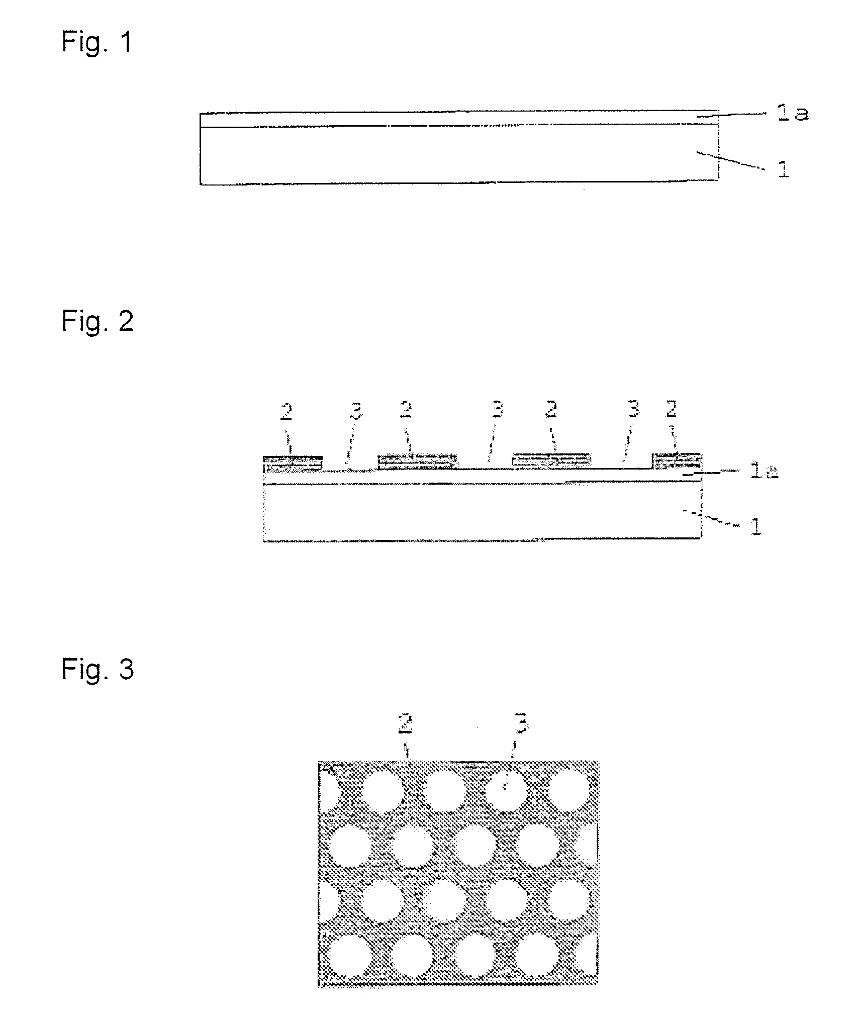
[0049]In a first embodiment, a starting substrate 1 (c-plane sapphire wafer, 2 inch or 50.8 mm diameter) is subjected to be grown by a 2 μm thick initial layer 1a of GaN by means of MOVPE (FIG. 1). Subsequently, this initial layer 1a is covered on the whole area by a 100 nm thick, sputtered mask layer 2 (WSiN layer) (FIG. 2). This layer 2 is structured by means of lithography and subsequent etching process such that hexagonally disposed circular openings 3 (windows) are formed (FIG. 3). In the example, hexagonally disposed circular windows (openings 3) having 10 μm diameter and a distance between central points of adjacent windows of 15 μm are used.

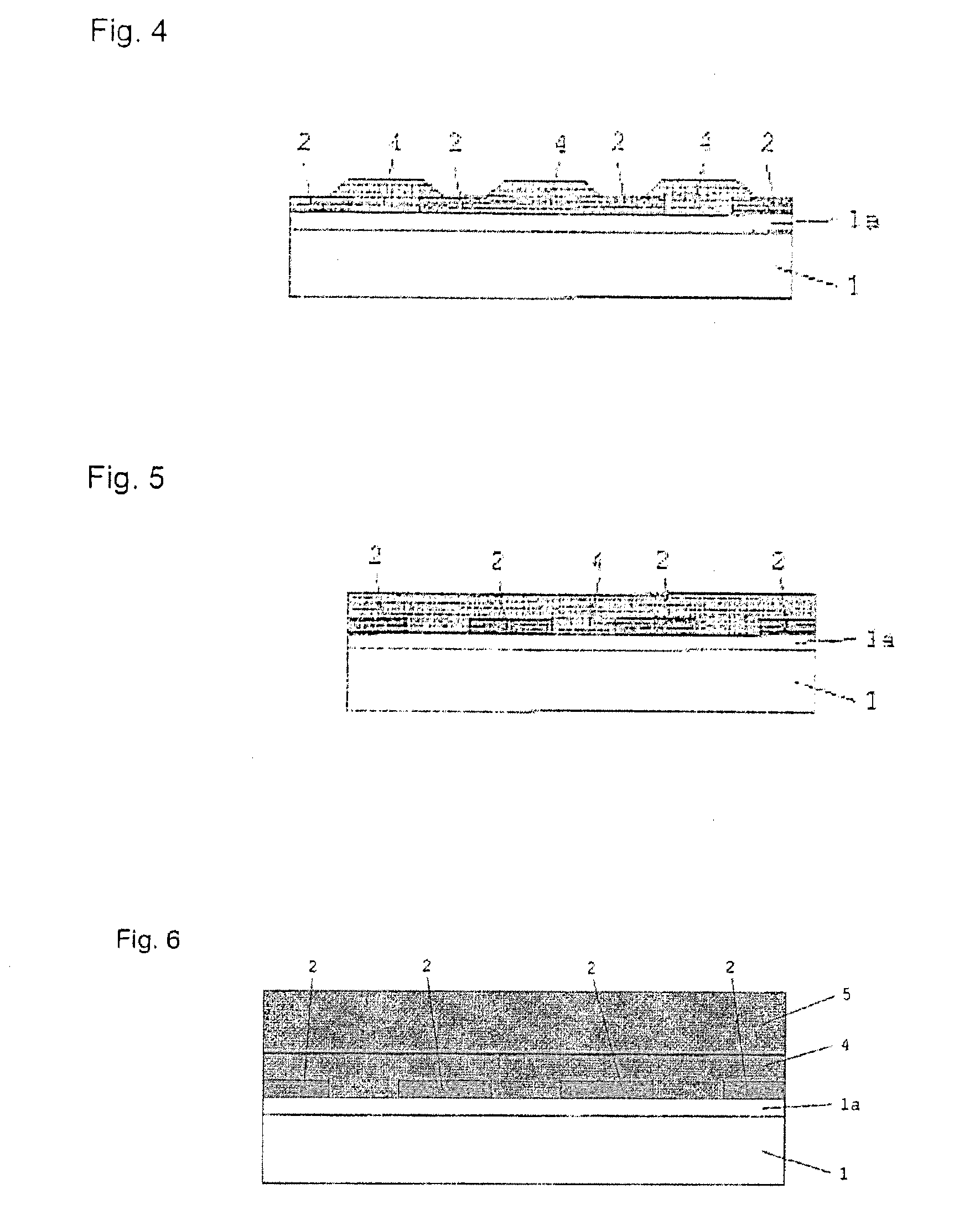
[0050]On the thus structured starting substrate, firstly a first semiconductor layer 4 of GaN is then grown as a coalescence layer (FIG. 4 and FIG. 5). Here, the starting substrate 1 with the initial layer 1a, being structured with the mask layer 2 and the openings 3, is heated in a horizontal HVPE reactor up to 1,040° C., wherein the sur...

second embodiment

[0051]In a second embodiment, a starting substrate 1 (c-plane sapphire substrate, diameter 50.8 mm) is subjected to be overgrown with a 2 μm thick GaN initial layer 1a by means of MOVPE (FIG. 1). Subsequently, this initial layer is covered over the whole area by a 100 nm thick, sputtered mask layer 2 (WSiN-layer) (FIG. 2). This layer is structured by means of lithography and subsequent etching process such that parallel extending stripes (openings 3) are formed. It is therefore used as a stripe mask.

[0052]The thus structured starting wafer 1, 2 is then overgrown with GaN by means of MOVPE such that islands growing out of the windows coalesce (FIG. 4 / 5). After coalescence is completed, on the obtained coherent GaN layer 4, a layer 5 made of GaN, AlN or AlGaN having a thickness above 50 μm is grown with a process suitable for enabling high growth rates, wherein thicknesses above 200 μm are advantageous (FIG. 6). The stress occurring during growth between the starting substrate 1 and t...

third embodiment

[0053]In a third embodiment, a starting substrate 1 of SiC is used, and a prior deposition of an initial layer 1a is omitted. The SiC-wafer 1 is directly covered by the 100 nm thick, sputtered mask layer 2 (WSiN-layer). This layer 2 is structured by means of lithography and subsequent etching process such that hexagonally disposed, circular openings 3 (windows) are formed (FIG. 3).

[0054]The thus structured starting wafer 1, 2 is then overgrown with GaN by means of MOVPE such that islands growing out of the windows do coalesce. After coalescence is completed, a second semiconductor layer 5 of GaN, AlN or AlGaN having a thickness above 50 μm is grown on the obtained coherent GaN layer 4 by a process suitable for enabling high growth rates, wherein thicknesses above 200 μm are advantageous. The stress occurring during growth between the starting substrate 1 and the grown semiconductor substrate 6—consisting of the first semiconductor layer 4, the coalescence layer, and the thick, secon...


PUM

PropertyMeasurementUnit
thicknessaaaaaaaaaa
thicknessaaaaaaaaaa
diametersaaaaaaaaaa

Abstract

The invention relates to a free-standing semiconductor substrate as well as a process and a mask layer for the manufacture of a free-standing semiconductor substrate, wherein the material for forming the mask layer consists at least partially of tungsten silicide nitride or tungsten silicide and wherein the semiconductor substrate self-separates from the starting substrate without further process steps.

Description

FIELD OF THE INVENTION[0001]The present invention relates to a semiconductor substrate as well as a process and a mask layer for the manufacture of a free-standing semiconductor substrate by means of hydride vapour phase epitaxy, in particular a process for the manufacture of free-standing gallium nitride (GaN)-, aluminum nitride (AlN)- and aluminum gallium nitride (AlGaN)-, indium nitride (InN)- and indium gallium nitride (InGaN)-substrates by means of hydride vapour phase epitaxy (HVPE), in which the semiconductor layer self-separates from a substrate (or starting / original substrate or foreign substrate) without further process steps.BACKGROUND OF THE INVENTION[0002]This self-separation is achieved through lateral epitaxial growth (ELO, Epitaxial Lateral Overgrowth) over a mask, wherein the mask is provided with openings (windows). In these windows, preferably a thin initial layer (or also starting layer) is uncovered, which had been grown on a substrate (such as, e.g., sapphire) ...

Claims


Application Information

Patent Timeline
Patent Type & Authority Patents(United States)
IPC IPC(8): C30B25/04H01L33/32
CPCH01L21/0237H01L21/02378H01L21/0242H01L21/02458H01L21/02502H01L21/0254H01L21/02581H01L21/0262H01L21/02642H01L21/02647H01L21/20
Inventor HENNIG, CHRISTIANWEYERS, MARKUSRICHTER, EBERHARDTRAENKLE, GUENTHER
Owner FREIBERGER COMPOUND MATERIALS
Why Eureka
Try Eureka