Carbon nanotubes, substrate and electron emission device with such carbon nanotubes and carbon nanotube synthesizing substrate as well as methods of and apparatus for making them

a carbon nanotube and electron emission technology, which is applied in the manufacture of electrode systems, metal/metal-oxide/metal-hydroxide catalysts, electric discharge tubes/lamps, etc., can solve the problems of inability to synthesize carbon nanotubes randomly aligned and then mechanically, and no reproducible method, etc., to achieve good electron emission efficiency, improve the effect of electron emission efficiency and good crystal quality

Inactive Publication Date: 2013-10-15
NAT INST FOR MATERIALS SCI +1
View PDF18 Cites 0 Cited by
  • Summary
  • Abstract
  • Description
  • Claims
  • Application Information

AI Technical Summary

Benefits of technology

[0050]According to synthesizing methods of carbon nanotubes of the present invention, carbon nanotubes having an excellent crystal quality, that there are little lattice defects such as disorders in carbon lattices arrangement and carbon vacancies, can be synthesized. It is also possible to realize providing an electron emission device extremely higher in electron emission efficiency than those in the prior art.
[0051]According to a substrate with carbon nanotubes, an electron emission device using the substrate and methods of making them, a substrate with carbon nanotubes which are highly oriented, densely aligned and have high a crystal quality can be used to realize providing an electron emission device which is extremely higher in electron emission efficiency than those in the prior art. According to an electron emission device of the present invention, the driving voltage therefor can be reduced and a current value that is sufficient to emit a fluorescent material on the market for slow electrons can be obtained. Moreover, an electron emission device of the present invention needs no gate electrode and can thus simplify the structure and reduce the cost of a surface light-emitting device for which the device is used. Further, the carbon material remains unoxidized even in a low vacuum and thus allows realizing a light emitting device that can be paneled more easily, and is longer in operating life than those using a conventional electron emission device.
[0052]According to a carbon nanotube synthesizing apparatus of the present invention, carbon nanotubes oriented normal to the substrate can be synthesized reproducibly and an electron emission device having high electron emission efficiency can be manufactured.

Problems solved by technology

Also, an oxide such as of metal or silicon by its insulating nature is hard to emit electrons.
As is well known, however, many conventional nanocarbon materials made by utilizing plasma contain a lot of impurity components such as amorphous substances and there has been no method that can reproducibly make highly aligned carbon nanotubes especially suitable to emit electrons uniformly.
Since carbon nanotubes are a nano material having a radius in the order of nanometers, it is impossible to synthesize carbon nanotubes randomly aligned and then to mechanically orient the individual carbon nanotubes and align them densely.

Method used


Image

  • Carbon nanotubes, substrate and electron emission device with such carbon nanotubes and carbon nanotube synthesizing substrate as well as methods of and apparatus for making them
  • Carbon nanotubes, substrate and electron emission device with such carbon nanotubes and carbon nanotube synthesizing substrate as well as methods of and apparatus for making them
  • Carbon nanotubes, substrate and electron emission device with such carbon nanotubes and carbon nanotube synthesizing substrate as well as methods of and apparatus for making them

Examples


example 1

[0131]Mention is next made of Example 1.

[0132]As the base substrate, a n-type Si (100) oriented substrate (having a specific resistance of 0.0026 Ω·cm and a size of 7×22×0.5 mm) was used.

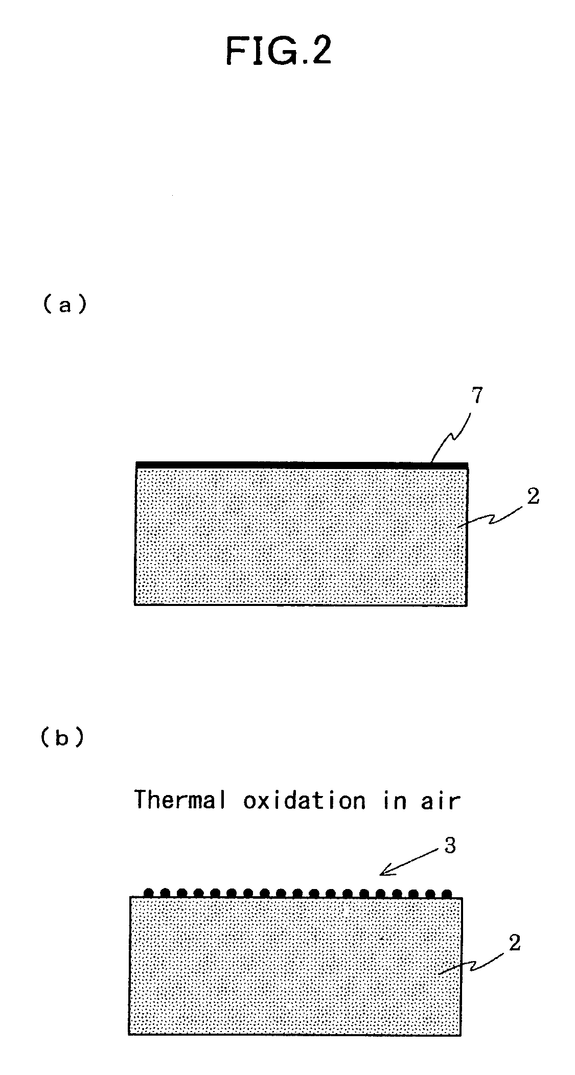
[0133]Initially, a cobalt thin film was deposited onto this substrate to a thickness of about 6 nm by magnetron sputtering and the substrate was then thermally oxidized in air at 900° C. for 10 minutes.

[0134]Then, in the apparatus shown in FIG. 7 carbon nanotubes were synthesized thereon by solid-liquid interfacial contact cracking in organic liquid in the apparatus as shown in FIG. 7.

[0135]Synthesis conditions used for solid-liquid interfacial contact cracking in an organic liquid are as follows:

[0136]Source organic liquid: methanol (purity of 99.9% and boiling point of 64.7° C.);

[0137]Synthesis temperature: 600° C.; and

[0138]Synthesis time: 5 minutes.

[0139]FIG. 4 is a chart illustrating X-ray photoelectron spectra for a thin film of cobalt before heat treatment in air at 900° C. for 10 minutes and...

example 2

[0151]Example 2 on a method of synthesizing carbon nanotubes in accordance with the present invention will be mentioned.

[0152]First, a cobalt thin film of 5 nm was deposited on a conductive silicon substrate by sputtering a cobalt target in an argon (Ar) atmosphere of 7 Pa with a discharge current of 35 mA for 3 minutes.

[0153]Then, the substrate was thermally oxidized to make a silicon conductive substrate carrying ultra-fine particles of cobalt oxide. The conditions for thermal oxidation were 900° C. and 15 minutes of heating by current passage in air. This thermal oxidation step was carried out in a way as mentioned in connection with FIG. 2 and is characterized in that in making densely aligned and highly oriented carbon nanotubes synthesizing substrate, a cobalt thin film deposited on a silicon or diamond substrate or a cobalt thin film deposited on a substrate comprising a glass, semiconductor, metal or oxide substrate and a silicon or diamond film formed thereon is thermally o...

example 3

[0162]Example 3 on an electron emission device of the present invention will be mentioned next.

[0163]An electron emission device using carbon nanotubes made in the Example of the carbon nanotube synthesizing according to the method of the present invention and an electron emission device using carbon nanotubes according to the conventional method were compared on their electron emission efficiencies.

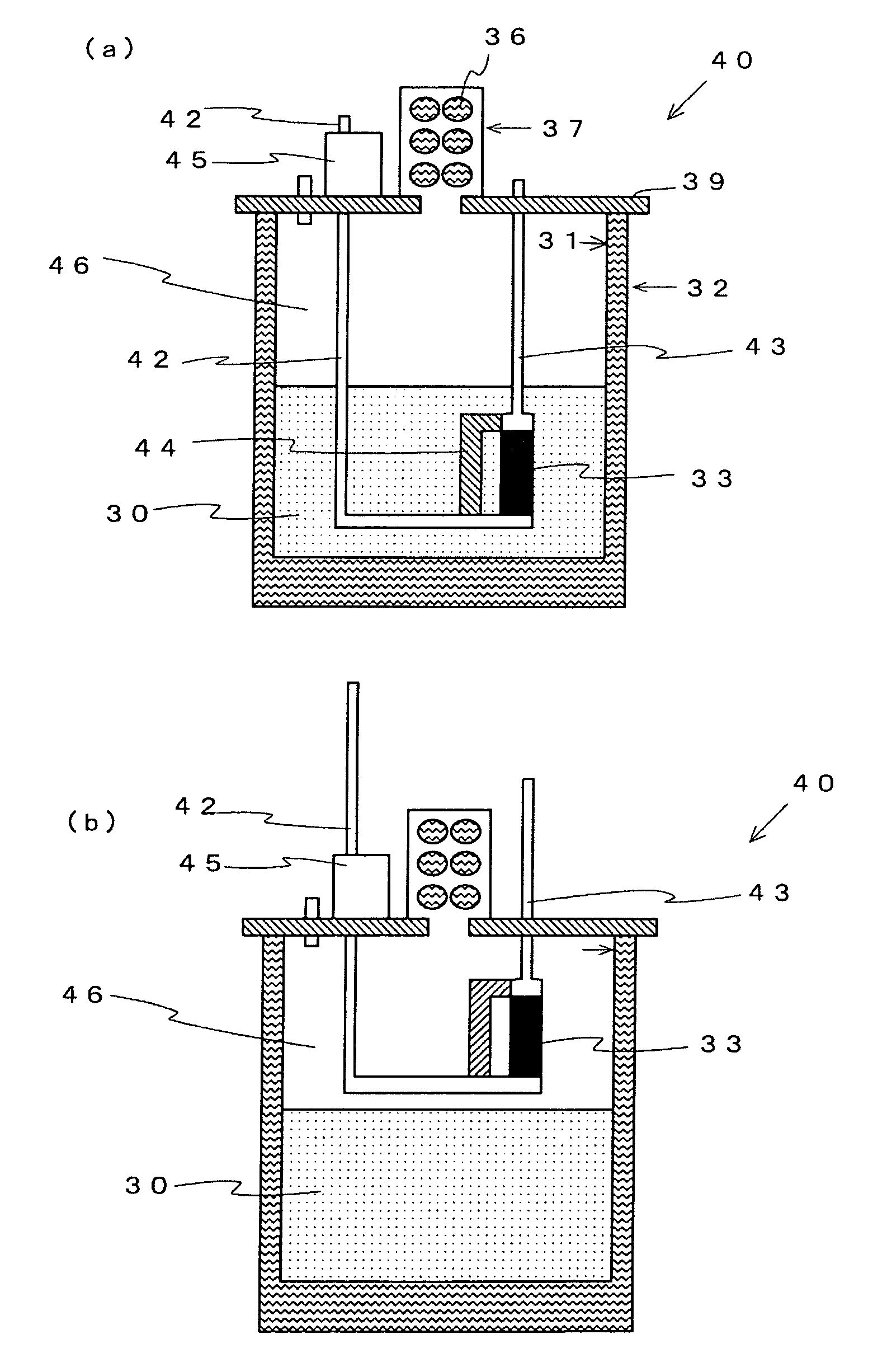
[0164]FIG. 9 is a diagram illustrating the structure of a device and a measuring circuit used in the measurement of electron emission efficiency. A conductive Si substrate 21 having carbon nanotubes 20 grown thereon was opposed via a spacer 22 to a glass substrate 23 having a transparent ITO (indium-tin-oxide film) electrode 23a vapor deposited thereon. And, with a voltage applied between the substrate 21 and the transparent electrode 23a, electric current flown between them was measured as a function of applied voltage. The carbon nanotubes 20 had their apical ends spaced from the trans...


PUM

PropertyMeasurementUnit
temperatureaaaaaaaaaa
time periodaaaaaaaaaa

Abstract

A novel carbon nanotube (64) is featured in that it has the highest Raman scattering intensity in the vicinity of 1580 cm−1 in its Raman spectrum. Carbon nanotubes can be grown on and from the catalytic fine particles (63) which consist of ultra-fine particles of cobalt oxide catalyst onto a substrate comprising a conductive substrate (62) and fine particles (63) of catalyst formed on a surface thereof. An electron emission device (60) so configured as to emit electrons by applying a voltage to apical ends (64a) of such carbon nanotubes (64) can be reduced in driving voltage and can achieve a current such as to emit a fluorescent material on the market for low-velocity electron beams. The electron emission device (60) needs no gate and can thus simplify the structure and reduce the cost of a surface light-emitting device for which the element is used. The carbon material remains unoxidized even in a low vacuum and thus allows realizing a light emitting device that can be paneled more easily, and is longer in operating life than those using a conventional electron emission device.

Description

TECHNICAL FIELD[0001]The present invention relates to a substrate and an electron emission device provided with carbon nanotubes which are densely aligned and highly oriented, and a substrate on which to synthesize the carbon nanotubes as well as methods of and apparatus for making them. More specifically, the present invention relates to a substrate with carbon nanotubes, methods of synthesizing carbon nanotubes suitable for synthesizing said substrate with carbon nanotubes, apparatus for making carbon nanotubes, a substrate on which to synthesize the carbon nanotubes, methods of making a substrate on which to synthesize the carbon nanotubes and an electron emission device using the substrate with carbon nanotubes.BACKGROUND ART[0002]In a conventional micro fabricated electron emission device, metals, silicon and their compounds as for materials of the device have been used. Such a material on its uppermost surface as the electron emission face becomes easily oxidized in air, formi...

Claims


Application Information

Patent Timeline
Patent Type & Authority Patents(United States)
IPC IPC(8): D01F9/12H01J1/02B32B7/00C25D17/00C25D9/04B05D3/02B32B5/16B32B15/04B32B9/00B32B17/06
CPCB01J35/002B01J35/0033B01J37/14B82Y10/00B82Y30/00C01B31/0233H01J1/304H01J9/025B82Y40/00B01J23/75Y10T428/24174H01J2201/30469Y10T428/30Y10T428/256C01B32/162B82B3/0004
Inventor ANDO, TOSHIHIRONAKAGAWA, KIYOHARUGAMO, MIKAGAMO, HIDENORI
Owner NAT INST FOR MATERIALS SCI
Why Eureka
Try Eureka