
Resistive random access memory using rare earth scandate thin film as storage medium

Active Publication Date: 2013-05-21
NAT TAIWAN UNIV OF SCI & TECH
View PDF1 Cites 4 Cited by
  • Summary
  • Abstract
  • Description
  • Claims
  • Application Information

AI Technical Summary

Benefits of technology

This patent describes a resistive random access memory (RRAM) that uses a rare earth scandate thin film as the storage medium and an amorphous rare earth scandate layer as the resistive memory layer. The technical effects of this invention include low operation voltage and low power consumption, as well as the capability for easy manufacturing without any thermal annealing or forming processes. Additionally, the use of rare earth scandate layers can provide high resistance state and low resistance state performance through unipolar resistance switching behavior.

Problems solved by technology

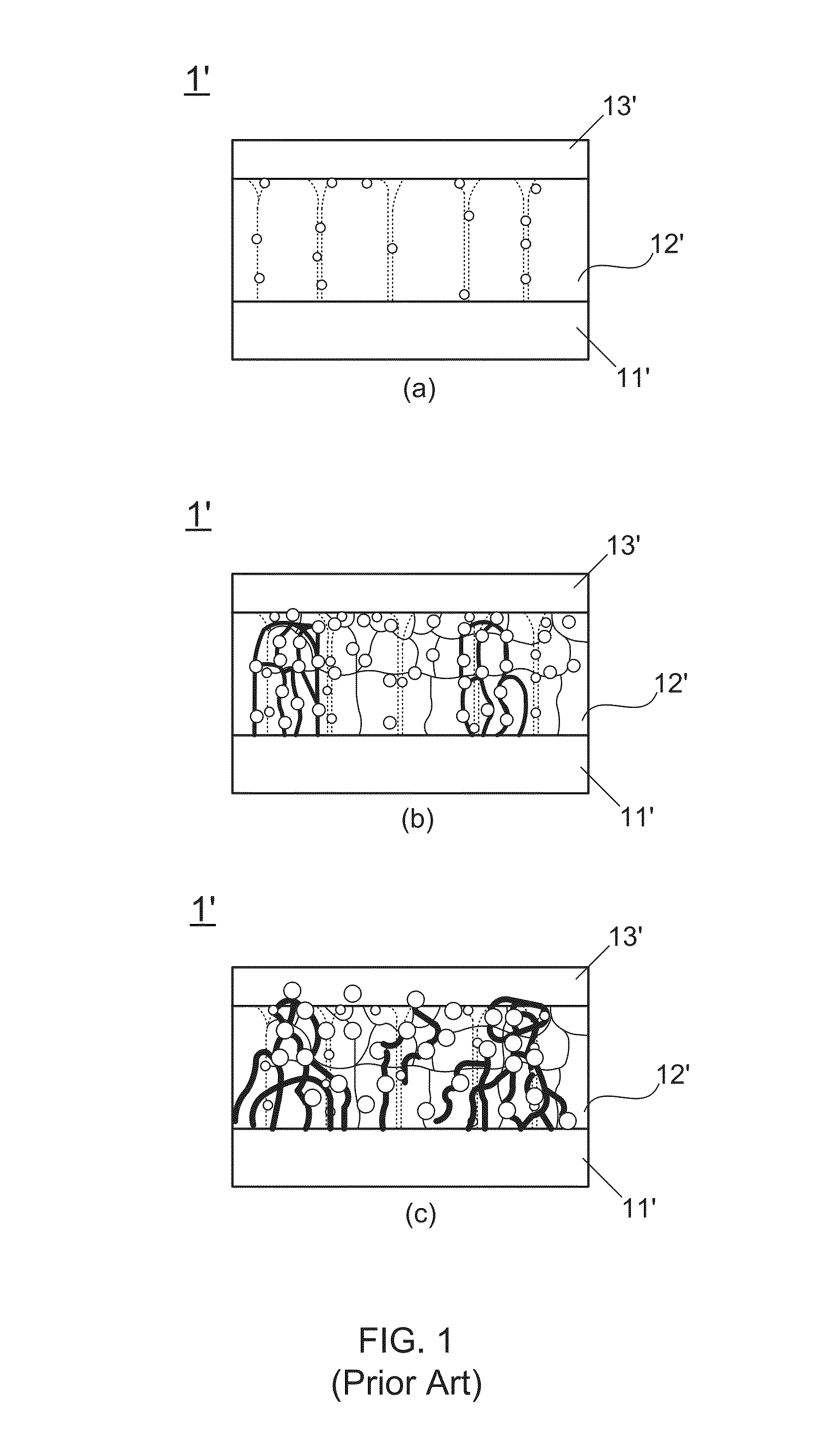
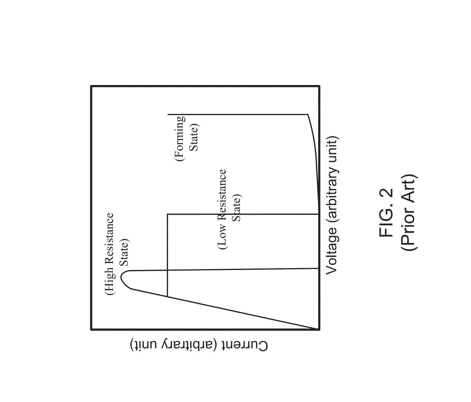
1. For making the aforesaid resistive random access memory 1′ include the resistance conversion characteristic, it must complete the metal filaments forming procedure of the resistive random access memory 1′ in advance; however, the breakdown of the resistive memory layer 12′ may occur in the resistive random access memory 1′ when high voltage is applied to the resistive random access memory 1′.
2. Inheriting to above point 1, it would yield high power consumption when the high voltage is applied to the resistive random access memory 1′ for executing the metal filaments forming procedure. The high voltages applied may also result in the breakdown (failure) device.
3. Generally, the resistive random access memory 1′ needs to be executed a thermal annealing process after the resistive random access memory 1′ is fabricated; For this reason, the thermal budget of the resistive random access memory 1′ is very high. Such thermal annealing is one of possible causes that could lead to the device failure.

Method used


Image

  • Resistive random access memory using rare earth scandate thin film as storage medium
  • Resistive random access memory using rare earth scandate thin film as storage medium
  • Resistive random access memory using rare earth scandate thin film as storage medium

Examples


Embodiment Construction

[0027]To more clearly describe a resistive random access memory using the rare earth scandate thin film as the storage medium according to the present invention, embodiments of the present invention will be described in detail with reference to the attached drawings hereinafter.

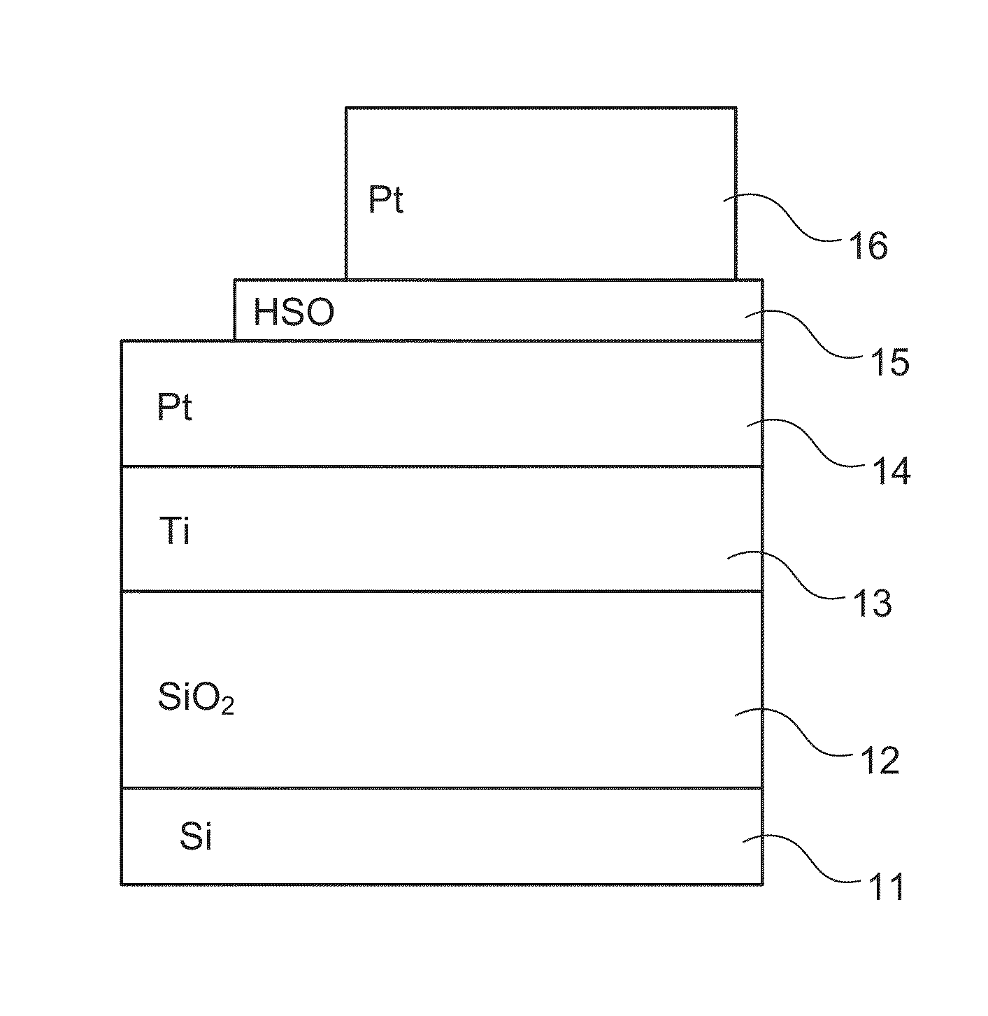
[0028]Please refer to FIG. 3, which illustrates a schematic framework diagram of a resistive random access memory using the rare earth scandate thin film as the storage medium according to the present invention. As shown in FIG. 3, the resistive random access memory 1 using rare earth scandate thin film as the storage medium includes: a substrate 11, an insulation layer 12, a first electrode layer 14, a resistive memory layer 15, and a second electrode layer 16. In the present invention, it uses a silicon-on-insulator (SOI) substrate for replacing the substrate 11 and the insulation layer 12, and the first electrode layer 14, the resistive memory layer 15 and the second electrode layer 16 are sequentially for...


PUM


Abstract

The present invention relates to a resistive random access memory using the rare earth scandate thin film as the storage medium, comprising a substrate, an insulation layer, a first electrode layer, a resistive memory layer, and a second electrode layer. In the present invention, it uses an amorphous rare earth scandate layer as the resistive memory layer of the resistive random access memory. Therefore, the resistive random access memory using the rare earth scandate thin film as the storage medium having advantages of low operation voltage and low power consumption can easily be manufactured without using any forming process or thermal annealing process. Moreover, through the characteristics of unipolar resistance switching behavior revealed by the amorphous rare earth scandate layer, the resistive random access memory using rare earth scandate thin film as the storage medium is able to perform a high resistance state and a low resistance state.

Description

BACKGROUND OF THE INVENTION[0001]1. Technical Field[0002]The present invention relates to a resistive random access memory, and more particularly, to a resistive random access memory using the rare earth scandate thin film as the storage medium.[0003]2. Description of Related Art[0004]With the evolution of the times, the development of technologies has a great progress. In particular, the digital electronic products are invented and widely used in human life. When using the electronic products, the electronic documents and digital data processed by the electronic products need to be stored in memories for caching or accessing. Generally, memories are divided into volatile memories and non-volatile memories, in which the new-generation non-volatile memories consist of ferroelectric random access memory (FeRAM), magnetoresistive random access memory (MRAM), phase-change random access memory (PRAM), and resistive random access memory (RRAM).[0005]In application, the resistive random ac...

Claims


Application Information

Patent Timeline
IPC IPC(8): H01L45/00
CPCG11C13/0007H01L45/04H01L45/147H01L45/1625H01L45/1253H10N70/20H10N70/841H10N70/8836H10N70/026
Inventor CHU, JINNCHANG, WEN-ZHI
Owner NAT TAIWAN UNIV OF SCI & TECH
Learn More