
Systems and methods for averaging error rates in non-volatile devices and storage systems

a non-volatile device and error rate technology, applied in memory systems, digital storage, instruments, etc., can solve the problems of storage interfaces that do not in themselves perform wear leveling, file metadata being constantly rewritten in-place, and space it uses is wear leveled

Active Publication Date: 2013-04-23
AVAGO TECH INT SALES PTE LTD
View PDF44 Cites 14 Cited by
  • Summary
  • Abstract
  • Description
  • Claims
  • Application Information

AI Technical Summary

Benefits of technology

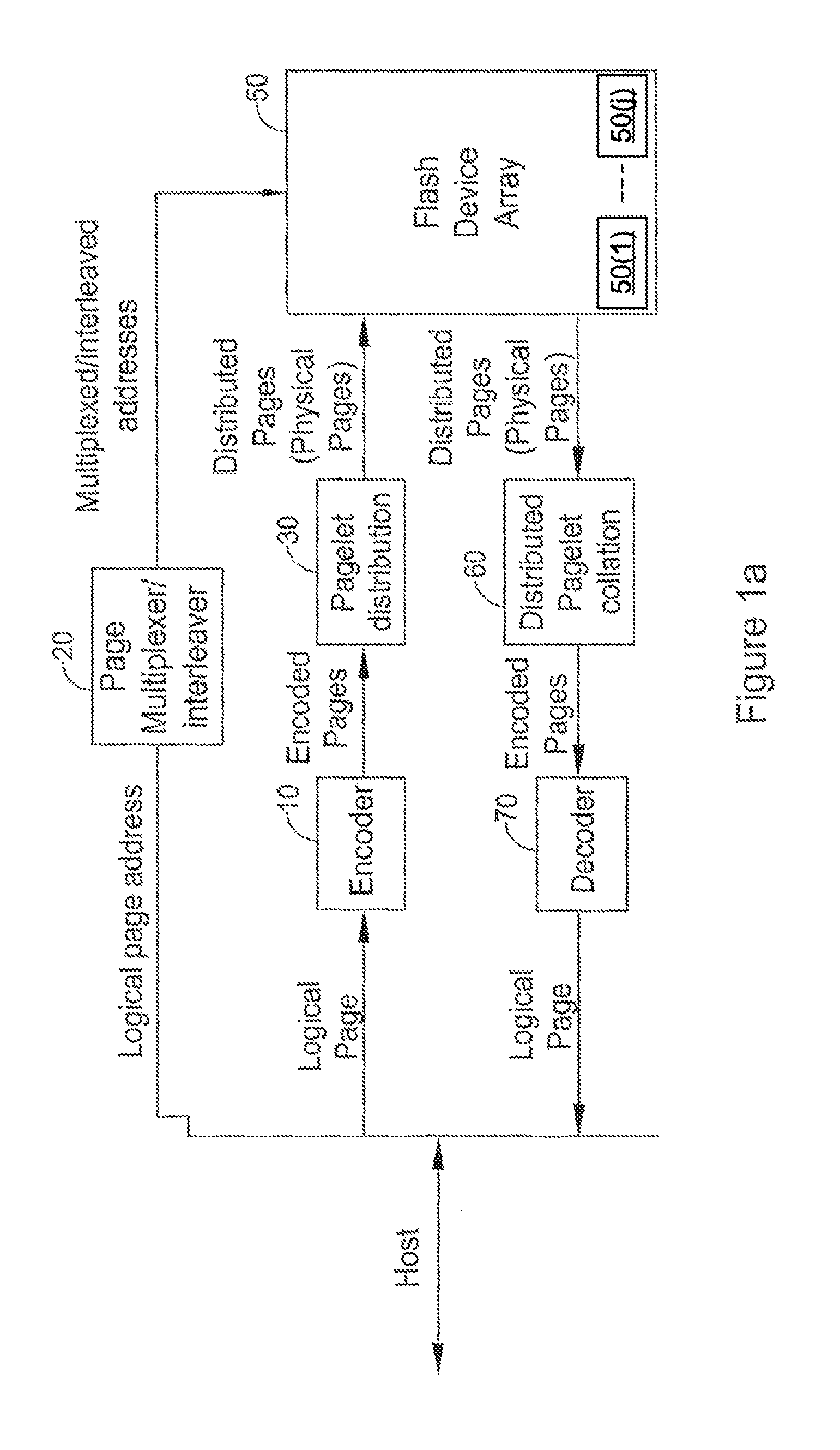
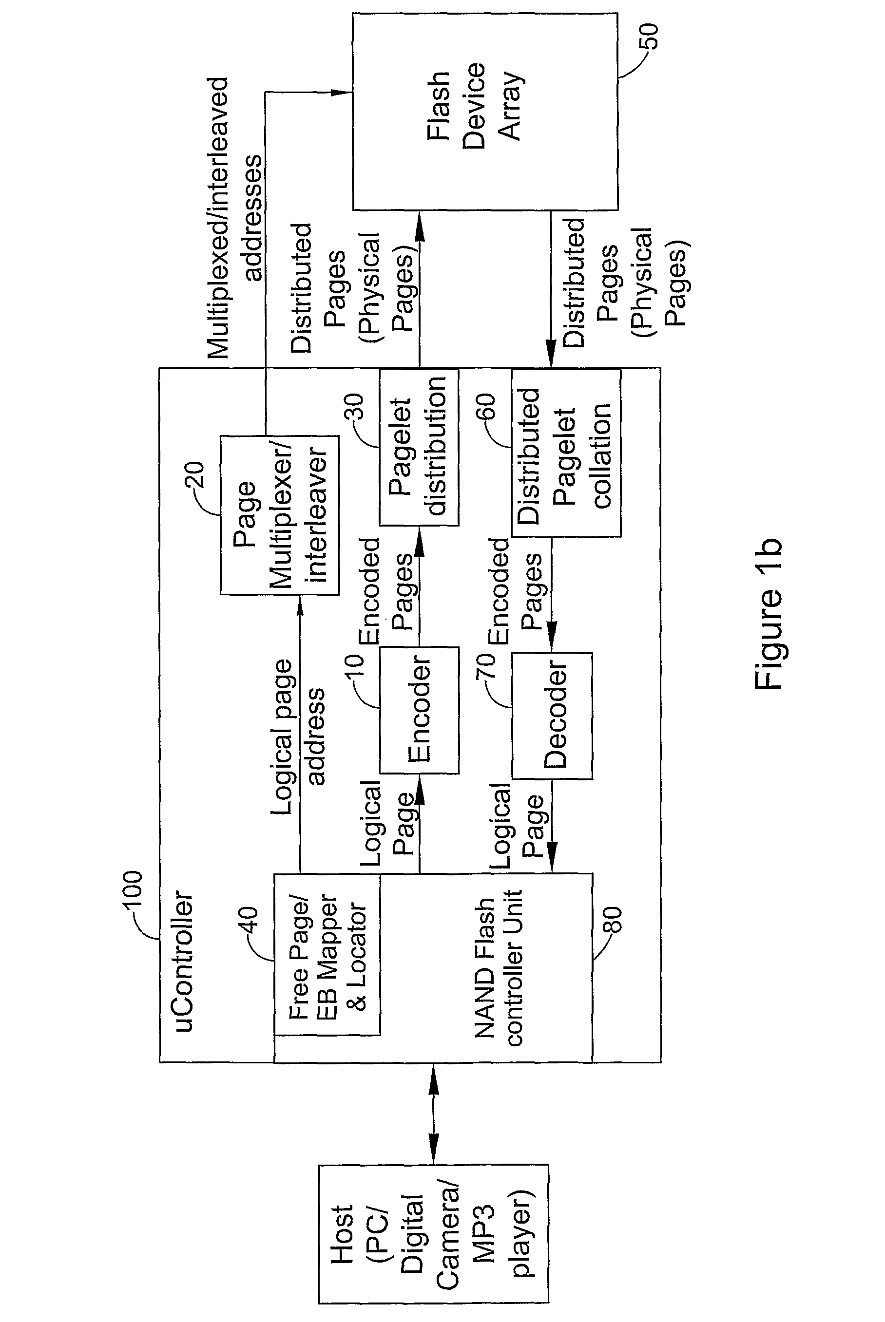
The present invention aims to mitigate the bit error rate (BER) problem by distributing each "logical" page across several physical pages in an erase block or across several devices. This results in an average bit error rate (BER) instead of the worst case BER. Additionally, the patent text provides methods for facilitating interaction between a data source supplying a stream of logical pages and a flash memory system with a multiplicity of physical pages or flash memory cells. The methods involve distributing data from each logical page in the stream between at least two of the physical pages or subsets of flash memory cells with different bit error rates to optimize program-erase performance.

Problems solved by technology

Some file systems aggravate the problem by tracking last-access times, which can lead to file metadata being constantly rewritten in-place.
The data structures for the queue itself must either be stored off-device or in such a way that the space it uses is itself wear-leveled.
Some storage interfaces do not in themselves perform wear leveling.”

Method used


Image

  • Systems and methods for averaging error rates in non-volatile devices and storage systems
  • Systems and methods for averaging error rates in non-volatile devices and storage systems
  • Systems and methods for averaging error rates in non-volatile devices and storage systems

Examples


Embodiment Construction

[0065]Today's Flash memory devices store information as charge in either a floating gate transistor or an NROM transistor. Multi-Level Cells (MLC) store several bits by setting the amount of charge in the cell. The amount of charge is then measured by a detector, e.g. by a threshold voltage of the cell's transistor gate. Due to inaccuracies during the multiple erase and programming procedures and because of charge loss due to time and temperature (also known as retention), the measured levels suffer from a random distortion. As a result, some errors appear when the device is read. This reliability is then measured by the error probability or by a bit error rate (BER).

[0066]Flash devices are organized into pages. Each page contains a section allocated for data (512 bytes-4Kbytes) and a small amount of bytes (16-32 bytes for every 512 data bytes) allocated for redundancy and back pointers. The redundancy bytes are used to store error correcting information, for correcting errors which...


PUM


Abstract

A system for storing a plurality of logical pages in a set of at least one flash device, each flash device including a set of at least one erase block, the system comprising apparatus for distributing at least one of the plurality of logical pages over substantially all of the erase blocks in substantially all of the flash devices, thereby to define, for at least one logical page, a sequence of pagelets thereof together including all information on the logical page and each being stored within a different erase block in the set of erase blocks; and apparatus for reading each individual page from among the plurality of logical pages including apparatus for calling and ordering the sequence of pagelets from different erase blocks in the set of erase blocks.

Description

CROSS-REFERENCE TO RELATED APPLICATIONS[0001]This application is a National Phase Application of PCT International Application No. PCT / IL2008 / 001238, entitled SYSTEMS AND METHODS FOR AVERAGING ERROR RATES IN NON-VOLATILE DEVICES AND STORAGE SYSTEMS, International Filing Date Sep. 17, 2008, published on Apr. 30, 2009 as International Publication No. WO 2009 / 053962 which in turns claims priority from U.S. Provisional Application No. 60 / 960,943, filed Oct. 22, 2007 and entitled “Systems and methods to reduce errors in Solid State Disks and Large Flash Devices” and U.S. Provisional Application No. 61 / 071,469, filed Apr. 30, 2008 and entitled “Systems and Methods for Averaging Error Rates in Non-Volatile Devices and Storage Systems”, all of which are incorporated herein by reference in their entirety.[0002]Other applications include: U.S. Provisional Application No. 60 / 960,207, filed Sep. 20, 2007 and entitled “Systems and Methods for Coupling Detection in Flash Memory”, U.S. Provisional...

Claims


Application Information

Patent Timeline
Patent Type & Authority Patents(United States)
IPC IPC(8): G11C11/34G11C16/04
CPCG06F11/1068G11C29/82G11C2029/0411
Inventor WEINGARTEN, HANAN
Owner AVAGO TECH INT SALES PTE LTD
Learn More